 ChipApex | Global Electronic Components Supplier

SEARCH
Search Product
Search Post
— IC芯片 | 连接器 | 传感器 | 被动器件 —
Search productSearch post
— IC芯片 | 连接器 | 传感器 | 被动器件 —
Consult the customer manager about the wholesale price.
consultation hotline:86-132-6715-2157
email:[email protected]
Contact the product manager for consultation. One-stop consultation is available.
Do you want a lower wholesale price? Please send us your inquiry and we will reply immediately.
74AHCT07APWJ is listed in the Buffers, Drivers, Receivers, Transceivers range at ChipApex. The manufacturer field lists Nexperia USA Inc.. Its product description is IC BUF NON-INVERT 5.5V 14TSSOP. Review the specifications below when checking this part for your BOM.
The Nexperia 74AHCT07APWJ is a hex buffer with open-drain outputs designed for operation within a supply voltage range of 4.5 V to 5.5 V. It features TTL-compatible inputs and Schmitt-trigger action for noise immunity. The device supports mixed-mode voltage operation, allowing translation from 3.3 V to 5 V. Key electrical parameters include a typical propagation delay (tPZL) of 3.4 ns at 5 V, a low-level output voltage (VOL(p)) below 0.8 V at VCC = 5 V, and an operating temperature range from -40 °C to +125 °C.
Verify the specific ordering suffix against the manufacturer's official documentation to confirm package type and temperature range. Ensure the procurement channel sources genuine Nexperia components to guarantee compliance with the specified electrical characteristics and reliability standards outlined in the product data sheet.
Select this component when a hex buffer with open-drain outputs is required for 5 V logic applications. It is suitable for designs needing TTL compatibility and Schmitt-trigger inputs to handle noisy signals. Consider the TSSOP14 package constraints and the need for external pull-up resistors due to the open-drain output structure.
The 74AHCT07A belongs to the AHCT logic family, which combines high-speed CMOS performance with TTL-compatible inputs. This series is designed for 5 V applications where direct interfacing with TTL devices is necessary. The APWJ variant specifically denotes the TSSOP14 plastic thin shrink small outline package version.
Direct replacements must match the hex buffer open-drain specification and AHCT logic family. Verify pinout compatibility and ensure the substitute part supports the 4.5 V to 5.5 V supply range and -40 °C to +125 °C temperature specifications.
Yes, the device is designed to operate over a VCC range from 4.5 V to 5.5 V, and its TTL-compatible inputs allow it to be used to translate from 3.3 V to 5 V.
The IOFF circuitry provides partial power-down mode operation by disabling the output, which prevents damaging backflow current through the device when it is powered down.
Explore related parts through Logic, Integrated Circuits (ICs), all product categories, ChipApex homepage.
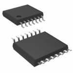 74AHCT07APWJ

The activity of extra discounts on wholesale prices is in full swing…
Please fill in your contact information and we will send you the latest wholesale price list.





