 ChipApex | Global Electronic Components Supplier

SEARCH
Search Product
Search Post
— IC芯片 | 连接器 | 传感器 | 被动器件 —
Search productSearch post
— IC芯片 | 连接器 | 传感器 | 被动器件 —
Consult the customer manager about the wholesale price.
consultation hotline:86-132-6715-2157
email:[email protected]
Contact the product manager for consultation. One-stop consultation is available.
Do you want a lower wholesale price? Please send us your inquiry and we will reply immediately.
74AHCT139D-Q100J is listed in the Signal Switches, Multiplexers, Decoders range at ChipApex. The manufacturer field lists Nexperia USA Inc.. Its product description is IC DECODER/DEMUX 1 X 2:4 16SO. Review the specifications below when checking this part for your BOM.
The Nexperia 74AHCT139D-Q100J is a dual 2-to-4 line decoder/demultiplexer in the 74AHCT logic family. It operates on a single power supply ranging from 4.5 V to 5.5 V and supports an ambient temperature range of -40 °C to +125 °C. The device features two independent decoders, each with two binary weighted address inputs (nA0, nA1) and one active LOW enable input (nE). It provides four mutually exclusive outputs (nY0 to nY3) per decoder. The component utilizes a 16-lead SO plastic small outline package (SOT109-1) with a body width of 3.9 mm.
Verify that the specific part number suffix matches the required package variant, as the datasheet lists both SO16 and TSSOP16 options under the same base model. Confirm the automotive grade designation aligns with project requirements. Ensure the ordering information corresponds to the correct temperature range specification before finalizing procurement orders.
Select this component when TTL-compatible input levels are required within a CMOS system architecture. The AHCT series ensures compatibility with standard TTL logic voltages while maintaining low power dissipation characteristics. Verify that the 5.5 V maximum input tolerance meets the interface requirements of the driving circuitry.
This device belongs to the Nexperia 74AHC/AHCT139-Q100 product family, which includes variants such as the 74AHC139D-Q100J and 74AHCT139PW-Q100. These components share identical functional descriptions but differ in input voltage thresholds and package types. The family is designed for robust performance in demanding automotive electronic applications requiring reliable signal decoding.
The 74AHC139D-Q100J serves as a CMOS-level compatible alternative within the same package. Cross-referencing requires verifying that the replacement device maintains the same 16-SOIC footprint and AEC-Q100 automotive qualification status.
In demultiplexer applications, the active LOW enable input (nE) acts as the data input. When enabled, the selected output follows the state of the enable pin, while other outputs remain HIGH.
The overvoltage tolerant inputs allow the device to be used as a translator between circuits operating at different voltage levels, specifically accepting input voltages up to 5.5 V even if the supply voltage is lower.
Explore related parts through Logic, Integrated Circuits (ICs), all product categories, ChipApex homepage.
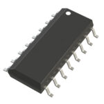 74AHCT139D-Q100J

The activity of extra discounts on wholesale prices is in full swing…
Please fill in your contact information and we will send you the latest wholesale price list.






