 ChipApex | Global Electronic Components Supplier
SEARCH
Search Product
Search Post
— IC芯片 | 连接器 | 传感器 | 被动器件 —
Search productSearch post
— IC芯片 | 连接器 | 传感器 | 被动器件 —
Consult the customer manager about the wholesale price.
consultation hotline:86-132-6715-2157
email:[email protected]
Contact the product manager for consultation. One-stop consultation is available.
Do you want a lower wholesale price? Please send us your inquiry and we will reply immediately.
The 74AHCT1G04SE-7 is a single inverter gate from the 74AHCT logic family, manufactured by Diodes Incorporated. It operates within a supply voltage range of 4.5V to 5.5V and features a standard totem pole output capable of ±8 mA drive current at 5.0V. The device utilizes Schmitt trigger inputs for tolerance against slow input transitions. It is housed in an SOT353 package with five pins: NC, A (Input), GND, Y (Output), and VCC. Propagation delay ranges from 0.6 ns to 8.5 ns depending on load capacitance and temperature.
Verify that the component matches the specific SE suffix indicating the SOT353 package configuration. Confirm the -7 suffix corresponds to tape and reel packaging quantities as specified in the ordering information. Ensure compatibility with the required 4.5V to 5.5V operating voltage range for AHCT logic families. Check for RoHS compliance and lead-free finish requirements relevant to your assembly process.
Select this component when a single inverter function is required with TTL-compatible input levels due to the AHCT designation. The inclusion of Schmitt triggers makes it suitable for noisy environments or applications with slow signal edges. Consider the SOT353 package size constraints and the ±8 mA output drive capability relative to the load requirements. Verify thermal resistance values if operating near maximum temperature limits.
This part belongs to the 74AHCT1G series of single-gate logic devices designed for 5V operation. It serves as a fundamental building block for digital logic inversion within systems requiring CMOS low power consumption combined with TTL-compatible input thresholds. The device is part of Diodes Incorporated's portfolio of surface-mount logic ICs intended for space-constrained portable and consumer electronics applications.
The datasheet does not list specific public substitute part numbers. Cross-reference with other manufacturers offering 74AHCT1G04 equivalents in SOT353 packages. Verify pinout compatibility, specifically the NC, Input, Ground, Output, and VCC arrangement. Ensure electrical characteristics such as propagation delay and output drive current meet or exceed the original specifications.
The Schmitt trigger action at all inputs makes the circuit tolerant for slower input rise and fall times, ensuring clean switching even with gradual signal transitions.
The device provides ESD protection exceeding 200-V Machine Model (A115-A), 2000-V Human Body Model (A114-A), and 1000-V Charged Device Model (C101C) per JESD 22 standards.
Unused inputs should be held at VCC or Ground to prevent undefined states and ensure proper operation.
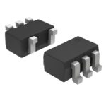 74AHCT1G04SE-7
The activity of extra discounts on wholesale prices is in full swing…
Please fill in your contact information and we will send you the latest wholesale price list.




