 ChipApex | Global Electronic Components Supplier

SEARCH
Search Product
Search Post
— IC芯片 | 连接器 | 传感器 | 被动器件 —
Search productSearch post
— IC芯片 | 连接器 | 传感器 | 被动器件 —
Consult the customer manager about the wholesale price.
consultation hotline:86-132-6715-2157
email:[email protected]
Contact the product manager for consultation. One-stop consultation is available.
Do you want a lower wholesale price? Please send us your inquiry and we will reply immediately.
74AHCT1G126GW,165 is listed in the Buffers, Drivers, Receivers, Transceivers range at ChipApex. The manufacturer field lists Nexperia USA Inc.. Its product description is IC BUF NON-INVERT 5.5V 5TSSOP. Review the specifications below when checking this part for your BOM.
The Nexperia 74AHCT1G126GW,165 is a single non-inverting buffer and line driver featuring three-state outputs. It operates within a supply voltage range of 4.5 V to 5.5 V and utilizes TTL input levels. The device provides symmetrical output impedance and balanced propagation delays. It is housed in a TSSOP5 plastic thin shrink small outline package (SOT353-1) with five leads and a body width of 1.25 mm. The component is specified for ambient temperatures ranging from -40 °C to +125 °C.
Verify the specific ordering suffix against official Nexperia documentation to confirm the exact tape-and-reel packaging configuration and manufacturing lot details. Ensure that the procurement channel sources components directly from authorized distributors to guarantee authenticity and traceability throughout the supply chain.
Select this component when a single-channel non-inverting buffer with three-state control is required for 5 V logic systems. The AHCT variant ensures compatibility with TTL input thresholds while maintaining CMOS performance. Verify that the operating temperature range and package dimensions align with the target PCB layout constraints.
This part belongs to the Nexperia 74AHC(AHCT)1G126 series of single bus buffers. The series offers various package options including XSON and SC-74A formats. The GW suffix specifically designates the TSSOP5 package type, distinguishing it from other physical form factors available within the same logical family.
Direct replacements include the 74AHCT1G126GV (SC-74A package) and the 74AHCT1G126GM (XSON6 package). These alternatives share identical electrical specifications but differ in physical footprint and pinout orientation.
The OE pin serves as the output enable input. When driven HIGH, the output assumes a high-impedance OFF-state regardless of the data input level.
The inputs are overvoltage tolerant up to 5.5 V, allowing the device to interface safely with higher voltage logic lines without damage or incorrect state interpretation.
Explore related parts through Logic, Integrated Circuits (ICs), all product categories, ChipApex homepage.
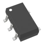 74AHCT1G126GW,165

The activity of extra discounts on wholesale prices is in full swing…
Please fill in your contact information and we will send you the latest wholesale price list.





