 ChipApex | Global Electronic Components Supplier

SEARCH
Search Product
Search Post
— IC芯片 | 连接器 | 传感器 | 被动器件 —
Search productSearch post
— IC芯片 | 连接器 | 传感器 | 被动器件 —
Consult the customer manager about the wholesale price.
consultation hotline:86-132-6715-2157
email:[email protected]
Contact the product manager for consultation. One-stop consultation is available.
Do you want a lower wholesale price? Please send us your inquiry and we will reply immediately.
74AHCT1G126SE-7 is listed in the Buffers, Drivers, Receivers, Transceivers range at ChipApex. The manufacturer field lists Diodes Incorporated. Its product description is IC BUF NON-INVERT 5.5V SOT353. Review the specifications below when checking this part for your BOM.
The 74AHCT1G126SE-7 is a single non-inverting buffer with a 3-state output, designed for operation within a power supply range of 4.5V to 5.5V. It features Schmitt trigger action at all inputs and provides ±8 mA output drive at 5.0V. The device operates across an ambient temperature range of -40°C to +125°C. Propagation delay (tpd) from input A to output Y ranges from 0.6 ns to 9.5 ns depending on load capacitance and temperature. Supply current (ICC) is typically 1 µA at 25°C and up to 40 µA at maximum operating temperatures.
Verify the specific package suffix 'SE' corresponds to the SOT353 configuration required for your PCB layout. Confirm the '-7' suffix indicates tape and reel packaging containing 3000 units per reel. Ensure the design accommodates the 4.5V to 5.5V operating voltage range and verify thermal resistance values if operating near the upper temperature limits.
Select this component when a single-channel, non-inverting buffer with 3-state control is needed in a compact SOT353 footprint. The AHCT family ensures TTL-compatible input levels while maintaining CMOS low power consumption. Consider the propagation delay specifications under your specific load capacitance conditions to ensure signal integrity meets system timing requirements.
This part belongs to the 74AHCT logic series, which combines the speed of Advanced High-speed CMOS technology with TTL-compatible input thresholds. The '1G' designation indicates a single gate implementation, and the '126' function code specifies a non-inverting buffer with 3-state outputs. Diodes Incorporated manufactures this device using lead-free finish and RoHS-compliant processes.
The 74AHCT1G126W5-7 serves as a direct functional substitute utilizing the SOT25 package instead of SOT353. Both variants share identical electrical characteristics and pinout assignments. Verify physical footprint compatibility before swapping between the SE and W5 package codes.
When the OE pin is driven HIGH, the buffer functions normally based on the input A. When OE is driven LOW, the output Y enters a high impedance state regardless of the input level.
The device exceeds 200 V for the Machine Model (A115-A), 2000 V for the Human Body Model (A114-A), and 1000 V for the Charged Device Model (C101C).
Explore related parts through Logic, Integrated Circuits (ICs), all product categories, ChipApex homepage.
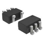 74AHCT1G126SE-7

The activity of extra discounts on wholesale prices is in full swing…
Please fill in your contact information and we will send you the latest wholesale price list.





