 ChipApex | Global Electronic Components Supplier

SEARCH
Search Product
Search Post
— IC芯片 | 连接器 | 传感器 | 被动器件 —
Search productSearch post
— IC芯片 | 连接器 | 传感器 | 被动器件 —
Consult the customer manager about the wholesale price.
consultation hotline:86-132-6715-2157
email:[email protected]
Contact the product manager for consultation. One-stop consultation is available.
Do you want a lower wholesale price? Please send us your inquiry and we will reply immediately.
74AHCT2G125DP,125 is listed in the Buffers, Drivers, Receivers, Transceivers range at ChipApex. The manufacturer field lists Nexperia USA Inc.. Its product description is IC BUF NON-INVERT 5.5V 8TSSOP. Review the specifications below when checking this part for your BOM.
The Nexperia 74AHCT2G125DP,125 is a dual buffer and line driver featuring three-state outputs controlled by active-low enable inputs (nOE). It operates within a supply voltage range of 4.5 V to 5.5 V and accepts TTL-level input signals. The device utilizes a TSSOP8 plastic thin shrink small outline package (SOT505-2) with an 8-lead configuration. Key electrical parameters include a maximum propagation delay of 8.5 ns at 5.5 V with a 50 pF load, a low-level output current capability of 8 mA, and a high-level output current of -8 mA. It functions reliably across an ambient temperature range of -40 °C to +125 °C.
Verify the specific ordering suffix
Select this component when interfacing TTL sources with CMOS loads requiring signal buffering. The AHCT series ensures compatibility with standard TTL voltage thresholds while offering the speed and drive strength of advanced CMOS technology. Ensure the design accommodates the 4.5 V minimum supply requirement and verify that the TSSOP8 thermal performance meets the application's power dissipation needs under maximum operating conditions.
This device belongs to the Nexperia 74AHC(AHCT)2Gxx family of dual-gate logic ICs designed for space-constrained applications. The 'DP' designation specifically identifies the TSSOP8 package variant, distinguishing it from other form factors like VSSOP8 or XSON8 within the same logical function family. These components are part of the broader 74-series logic ecosystem, providing standardized functionality for general-purpose digital logic circuits.
Direct functional equivalents include the 74AHC2G125DP for CMOS input level applications and the 74AHCT2G125DC for alternative packaging. Verify pinout compatibility and ensure the replacement maintains the required TTL input threshold specifications if used in mixed-voltage systems.
It functions as a dual non-inverting buffer with three-state outputs. When the enable pin is low, the input signal passes to the output; when high, the output enters a high-impedance state.
Yes, the inputs are overvoltage tolerant up to 5.5 V. This allows the device to translate signals from lower voltage domains into a 5 V system without damage, provided the supply voltage is maintained within the specified 4.5 V to 5.5 V range.
Explore related parts through Logic, Integrated Circuits (ICs), all product categories, ChipApex homepage.
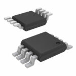 74AHCT2G125DP,125

The activity of extra discounts on wholesale prices is in full swing…
Please fill in your contact information and we will send you the latest wholesale price list.





