 ChipApex | Global Electronic Components Supplier

SEARCH
Search Product
Search Post
— IC芯片 | 连接器 | 传感器 | 被动器件 —
Search productSearch post
— IC芯片 | 连接器 | 传感器 | 被动器件 —
Consult the customer manager about the wholesale price.
consultation hotline:86-132-6715-2157
email:[email protected]
Contact the product manager for consultation. One-stop consultation is available.
Do you want a lower wholesale price? Please send us your inquiry and we will reply immediately.
74AHCT2G126GD,125 is listed in the Buffers, Drivers, Receivers, Transceivers range at ChipApex. The manufacturer field lists Nexperia USA Inc.. Its product description is IC BUFFER NON-INVERT 5.5V 8XSON. Review the specifications below when checking this part for your BOM.
The 74AHCT2G126GD,125 is a dual buffer and line driver featuring three-state outputs controlled by active-low output enable inputs. It operates within a supply voltage range of 4.5 V to 5.5 V and utilizes TTL input switching levels. The device provides symmetrical output impedance with high noise immunity and low power dissipation. Inputs are overvoltage tolerant, enabling use as translators in mixed-voltage environments. It is specified for operation from -40 °C to +125 °C and includes ESD protection exceeding 2000 V (HBM) and 1000 V (CDM).
Verify component authenticity through authorized Nexperia distributors or certified partners. Confirm the specific suffix GD indicates the 8-XSON package variant. Check current lifecycle status as this part may be discontinued; validate availability of equivalent alternatives if long-term supply is required. Ensure RoHS3 compliance matches project specifications.
Select this component when TTL-level inputs are required alongside CMOS performance characteristics. The AHCT series is appropriate for 5 V systems needing robust noise immunity. Consider the 8-XSON package for compact surface-mount designs. Verify that the 4.5 V minimum supply voltage aligns with the target system's power rails before finalizing the design.
This device belongs to the Nexperia 74AHC/AHCT family of high-speed Si-gate CMOS logic devices. It shares functional similarities with other buffers like the 74AHC2G126 but differs in input threshold requirements. The MicroPak™ packaging technology enables small form factors suitable for portable electronics and dense circuit boards.
The 74AHCT2G126DC,125 serves as a verified substitute offering identical electrical functionality in an 8-VSSOP package. Designers must account for pinout compatibility and thermal differences when transitioning between the XSON and VSSOP footprints during board redesigns.
The nOE pin is an active-low output enable input. When driven LOW, the outputs assume a high-impedance OFF-state, effectively disconnecting them from the bus.
Yes, the overvoltage tolerant inputs allow the device to accept signals higher than its own VCC, facilitating translation in mixed-voltage environments.
Explore related parts through Logic, Integrated Circuits (ICs), all product categories, ChipApex homepage.
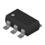 74AHCT2G126GD,125

The activity of extra discounts on wholesale prices is in full swing…
Please fill in your contact information and we will send you the latest wholesale price list.





