 ChipApex | Global Electronic Components Supplier

SEARCH
Search Product
Search Post
— IC芯片 | 连接器 | 传感器 | 被动器件 —
Search productSearch post
— IC芯片 | 连接器 | 传感器 | 被动器件 —
Consult the customer manager about the wholesale price.
consultation hotline:86-132-6715-2157
email:[email protected]
Contact the product manager for consultation. One-stop consultation is available.
Do you want a lower wholesale price? Please send us your inquiry and we will reply immediately.
74AHCT594S16-13 is listed in the Shift Registers range at ChipApex. The manufacturer field lists Diodes Incorporated. Its product description is AHC HIGH PIN COUNT SO-16. Review the specifications below when checking this part for your BOM.
The 74AHCT594S16-13 is an advanced high-speed CMOS device designed to be pin-compatible with 74LS low-power Schottky types. It functions as an 8-bit shift register with an 8-bit output register, accepting serial data from the DS input on each positive transition of the SHCP clock. The storage register captures data via the STCP pulse and asserts it on push-pull outputs Q0-Q7. It operates within a supply voltage range of 4.5V to 5.5V, sinks or sources 8mA at VCC=4.5V, and includes independent active-low reset functions for both registers.
Verify the specific package suffix 'S16' corresponds to the SO-16 footprint required for your PCB layout. Confirm that the -13 suffix indicates standard tape and reel packaging quantities. Ensure the design accommodates the 4.5V to 5.5V operating voltage range and check for any RoHS compliance documentation requirements specific to your region.
Select this component when pin compatibility with legacy 74LS devices is required alongside modern CMOS performance. It is suitable for designs needing independent control over shift and storage register resets. Consider the 8mA drive capability and wide input voltage tolerance if interfacing with varying signal levels within the specified supply constraints.
This part belongs to the 74AHCT series, representing advanced high-speed CMOS technology compatible with TTL logic levels. Diodes Incorporated manufactures this family to bridge legacy system interfaces with modern low-power requirements. The S16 designation specifically identifies the surface-mount SO-16 package variant within this product line.
Datasheet confirms pin compatibility with 74LS low-power Schottky types. Verify electrical characteristics such as propagation delay and drive current against original LS specifications to ensure functional equivalence in timing-critical circuits.
Data enters the shift register on the rising edge of SHCP. Data transfers to the storage register on the rising edge of STCP. Both registers have independent active-low reset inputs (SHR and STR).
Q7S provides a serial data output from the shift register, allowing information to be cascaded between multiple devices before it reaches the final parallel output register.
Explore related parts through Logic, Integrated Circuits (ICs), all product categories, ChipApex homepage.
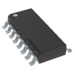 74AHCT594S16-13

The activity of extra discounts on wholesale prices is in full swing…
Please fill in your contact information and we will send you the latest wholesale price list.





