 ChipApex | Global Electronic Components Supplier

SEARCH
Search Product
Search Post
— IC芯片 | 连接器 | 传感器 | 被动器件 —
Search productSearch post
— IC芯片 | 连接器 | 传感器 | 被动器件 —
Consult the customer manager about the wholesale price.
consultation hotline:86-132-6715-2157
email:[email protected]
Contact the product manager for consultation. One-stop consultation is available.
Do you want a lower wholesale price? Please send us your inquiry and we will reply immediately.
74AHCV541APWJ is listed in the Buffers, Drivers, Receivers, Transceivers range at ChipApex. The manufacturer field lists Nexperia USA Inc.. Its product description is IC BUF NON-INVERT 5.5V 20TSSOP. Review the specifications below when checking this part for your BOM.
The Nexperia 74AHCV541APWJ is an octal buffer and line driver featuring three-state outputs, housed in a TSSOP20 (SOT360-1) package. It operates within a supply voltage range of 1.8 V to 5.5 V and supports mixed-mode voltage environments through overvoltage tolerant inputs. The device includes Schmitt trigger inputs for signal conditioning and IOFF circuitry for partial power-down applications. It provides two active-low output enables (OE1 and OE2) to control the high-impedance OFF-state.
Verify the specific suffix 'PWJ' against official Nexperia documentation to confirm it corresponds to the standard TSSOP20 package variant. Ensure compatibility with required temperature ranges (-40 °C to +125 °C) and check for any specific reel or cut-tape packaging requirements associated with this ordering code.
Select this component when an octal buffer with three-state outputs and Schmitt trigger inputs is required. It is suitable for designs needing mixed-voltage interface capabilities and partial power-down functionality. Verify that the TSSOP20 package fits the PCB layout constraints and that the 1.8 V to 5.5 V supply range matches the system design.
This part belongs to the 74AHCV541A family of octal buffers and line drivers. The 'PWJ' designation indicates the specific plastic thin shrink small outline package (TSSOP20) version manufactured by Nexperia. Other variants in this family include the DHVQFN20 package option.
The 74AHCV541ABQ serves as a pin-compatible alternative in a DHVQFN20 package. Verify thermal dissipation requirements and footprint compatibility before substitution.
The device utilizes IOFF circuitry which disables the outputs, preventing damaging backflow current through the device when it is powered down.
OE1 and OE2 are output enable inputs that are active LOW. A HIGH level on either pin causes the associated outputs to assume a high-impedance OFF-state.
Explore related parts through Logic, Integrated Circuits (ICs), all product categories, ChipApex homepage.
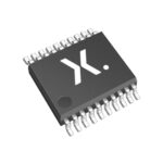 74AHCV541APWJ

The activity of extra discounts on wholesale prices is in full swing…
Please fill in your contact information and we will send you the latest wholesale price list.





