 ChipApex | Global Electronic Components Supplier
74ALVC08PW,118
Search Product
Search Post
— IC芯片 | 连接器 | 传感器 | 被动器件 —
Search productSearch post
— IC芯片 | 连接器 | 传感器 | 被动器件 —
Consult the customer manager about the wholesale price.
consultation hotline:86-132-6715-2157
email:[email protected]
Contact the product manager for consultation. One-stop consultation is available.
Do you want a lower wholesale price? Please send us your inquiry and we will reply immediately.
The Nexperia 74ALVC08PW,118 is a quad 2-input AND gate in the ALVC logic series. It operates within a supply voltage range of 1.65 V to 3.6 V and supports an ambient temperature range from -40 °C to +125 °C. The device utilizes Schmitt-trigger inputs for noise tolerance and includes IOFF circuitry for partial power-down protection. Propagation delay ranges from 1.0 ns to 3.7 ns depending on voltage and temperature. It is housed in a TSSOP14 (SOT402-1) package with 14 leads.
Verify the specific ordering suffix
Select this component when low power dissipation and high-speed operation are required alongside robust ESD protection. The ALVC series offers faster switching than standard LVC variants while maintaining compatibility with 3.3 V and 5 V systems. Ensure the design accounts for the specified propagation delays and power dissipation capacitance values under the intended load conditions.
This part belongs to the Nexperia 74ALVC family of advanced low-voltage CMOS logic gates. The 74ALVC08 specifically implements four independent 2-input AND functions. It is designed for high-speed digital applications where low power consumption and wide operating voltage ranges are critical constraints.
Direct pin-compatible alternatives include the 74ALVC08D (SO14 package) and 74ALVC08BQ (DHVQFN14 package). Verify that the substitute package type meets the mechanical footprint requirements of the target PCB design.
The IOFF circuitry automatically disables the outputs when the device is powered down (VCC = 0 V), preventing potentially damaging backflow current through the device.
The inputs are overvoltage tolerant up to 3.6 V, allowing them to interface directly with TTL levels even when the supply voltage is lower.
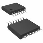 74ALVC08PW,118
The activity of extra discounts on wholesale prices is in full swing…
Please fill in your contact information and we will send you the latest wholesale price list.





