 ChipApex | Global Electronic Components Supplier
SEARCH
Search Product
Search Post
— IC芯片 | 连接器 | 传感器 | 被动器件 —
Search productSearch post
— IC芯片 | 连接器 | 传感器 | 被动器件 —
Consult the customer manager about the wholesale price.
consultation hotline:86-132-6715-2157
email:[email protected]
Contact the product manager for consultation. One-stop consultation is available.
Do you want a lower wholesale price? Please send us your inquiry and we will reply immediately.
The Nexperia 74ALVC16834ADGG,11 is an 18-bit registered driver featuring inverted register enable and 3-state outputs. It operates within a supply voltage range of 1.2 V to 3.6 V and supports direct interface with TTL levels at voltages from 2.7 V to 3.6 V. The device provides a current drive capability of ±24 mA at VCC = 3.0 V. Propagation delay ranges from 1.0 ns to 5.4 ns depending on the control signal and voltage. It utilizes a MULTIBYTE flow-through standard pin-out architecture in a TSSOP56 package.
Verify the specific ordering suffix against official documentation to confirm package type and temperature range. Confirm that the component meets JEDEC standards JESD8-5 and JESD8B/JESD36 for the intended operating voltage. Ensure design safeguards are implemented to manage ESD protection requirements as specified in the datasheet.
Select this component for designs requiring 18-bit registered driving with inverted register enable. It is suitable for applications needing direct TTL level interfacing and robust current drive capabilities. Verify that the operating temperature range of -40 °C to +85 °C aligns with system environmental constraints.
This part belongs to the 74ALVC16834A series of 18-bit registered drivers manufactured by Nexperia. It is housed in a TSSOP56 plastic thin shrink small outline package (SOT364-1). The device is designed for low-power CMOS consumption while maintaining high-speed performance through advanced BiCMOS technology.
Direct substitute: 74ALVCH16843DGGY
Operation of the OE input does not affect the state of the latch/flip-flop; it only controls whether the outputs are active or in a high-impedance OFF-state.
When LE is LOW, the A to Y data flow is transparent. When LE is HIGH and CP is held at LOW or HIGH, the data is latched.
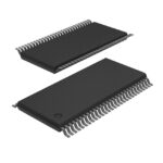 74ALVC16834ADGG,11
The activity of extra discounts on wholesale prices is in full swing…
Please fill in your contact information and we will send you the latest wholesale price list.






