 ChipApex | Global Electronic Components Supplier

SEARCH
Search Product
Search Post
— IC芯片 | 连接器 | 传感器 | 被动器件 —
Search productSearch post
— IC芯片 | 连接器 | 传感器 | 被动器件 —
Consult the customer manager about the wholesale price.
consultation hotline:86-132-6715-2157
email:[email protected]
Contact the product manager for consultation. One-stop consultation is available.
Do you want a lower wholesale price? Please send us your inquiry and we will reply immediately.
74ALVC573PW,112 is listed in the Latches range at ChipApex. The manufacturer field lists Nexperia USA Inc.. Its product description is IC D-TYPE TRANSP SGL 8:8 20TSSOP. Review the specifications below when checking this part for your BOM.
The Nexperia 74ALVC573PW,112 is an octal D-type transparent latch with 3-state outputs housed in a 20-TSSOP package. It operates within a supply voltage range of 1.65 V to 3.6 V and supports ambient temperatures from -40 °C to +125 °C. The device features Schmitt trigger inputs for slow signal tolerance and IOFF circuitry for partial power-down protection. Propagation delays (Dn to Qn) range from 1.0 ns to 6.2 ns depending on voltage, while output drive capabilities reach ±24 mA at 3.0 V.
Verify the specific ordering suffix ',112' against official Nexperia documentation to confirm tape-and-reel packaging specifications. Ensure the component meets RoHS3 compliance requirements for your region. Cross-reference the full part number with the manufacturer's latest product status to confirm active production availability before finalizing procurement plans.
Select this component when designing systems requiring high-speed data latching with low power consumption. The ALVC series offers superior speed compared to standard LVC devices. Ensure the design accommodates the specified input transition rates and utilizes the IOFF feature if partial power-down states are required in the system architecture.
This device belongs to the 74ALVC family of high-speed CMOS logic. It serves as an 8-bit storage element compatible with various low-voltage logic standards. The TSSOP20 package provides a compact solution for space-constrained designs while maintaining electrical performance suitable for modern embedded systems.
The 74ALVC573PW is the base package variant. Other packages include SO20 (74ALVC573D) and DHVQFN20 (74ALVC573BQ). Verify pin compatibility and thermal characteristics when substituting between package types.
The IOFF circuitry disables the outputs when the device is powered down, preventing potentially damaging backflow current through the device.
A HIGH on the OE input causes the outputs to assume a high-impedance OFF-state, but it does not affect the internal state stored in the latches.
Explore related parts through Logic, Integrated Circuits (ICs), all product categories, ChipApex homepage.
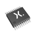 74ALVC573PW,112

The activity of extra discounts on wholesale prices is in full swing…
Please fill in your contact information and we will send you the latest wholesale price list.





