 ChipApex | Global Electronic Components Supplier
SEARCH
Search Product
Search Post
— IC芯片 | 连接器 | 传感器 | 被动器件 —
Search productSearch post
— IC芯片 | 连接器 | 传感器 | 被动器件 —
Consult the customer manager about the wholesale price.
consultation hotline:86-132-6715-2157
email:[email protected]
Contact the product manager for consultation. One-stop consultation is available.
Do you want a lower wholesale price? Please send us your inquiry and we will reply immediately.
The Nexperia 74ALVCH162601DGG is an 18-bit universal bus transceiver housed in a TSSOP56 package (SOT364-1). It operates within a supply voltage range of 1.65 V to 3.6 V and supports temperatures from -40 °C to +85 °C. The device features integrated 30 Ω termination resistors, bus hold inputs, and 3-state outputs. Data flow direction is controlled by OEAB/OEBA, LEAB/LEBA, CEAB/CEBA, and CPAB/CPBA inputs. Propagation delay ranges from 1.3 ns to 6.7 ns depending on the control signal and voltage.
Verify the specific ordering suffix matches the required package variant. Confirm that the application environment remains within the specified temperature range of -40 °C to +85 °C. Ensure supply voltage does not exceed the maximum rating of 3.6 V. Check for compliance with relevant JEDEC standards based on the operating voltage. Validate IOFF requirements if partial power down functionality is utilized in the design.
Select this component when an 18-bit wide bidirectional data path is required with integrated termination. The MULTIBYTE™ architecture simplifies PCB routing compared to discrete solutions. Consider the ALVCH family characteristics for low power consumption and direct TTL level interfacing capabilities. Evaluate the propagation delay specifications against the target system clock speeds to ensure timing margins are met.
This device belongs to the ALVCH logic family, designed for advanced low-voltage CMOS applications. It utilizes BiCMOS technology to achieve high speed while maintaining low power dissipation. The 74ALVCH162601 provides a standardized solution for wide data buses, integrating functions typically requiring external components into a single 56-lead package.
Check for 74ALVCH162601 variants with different suffixes for package or tape/reel options. Verify functional compatibility with other 18-bit universal bus transceivers if redesigning.
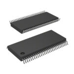 74ALVCH162601DGG:1
The activity of extra discounts on wholesale prices is in full swing…
Please fill in your contact information and we will send you the latest wholesale price list.






