 ChipApex | Global Electronic Components Supplier
SEARCH
Search Product
Search Post
— IC芯片 | 连接器 | 传感器 | 被动器件 —
Search productSearch post
— IC芯片 | 连接器 | 传感器 | 被动器件 —
Consult the customer manager about the wholesale price.
consultation hotline:86-132-6715-2157
email:[email protected]
Contact the product manager for consultation. One-stop consultation is available.
Do you want a lower wholesale price? Please send us your inquiry and we will reply immediately.
The SN74ALVCH162836VRE4 is a 20-bit universal bus driver with 3-state outputs manufactured by Texas Instruments. It operates within a supply voltage range of 1.65 V to 3.6 V and supports data rates up to 150 MHz. The device utilizes an EPIC submicron CMOS process and features active bus-hold circuitry on data inputs, eliminating the need for external pullup or pulldown resistors. It includes equivalent 26-ohm series resistors in the output port to reduce overshoot and undershoot without requiring external components. Designed for compliance with JEDEC SDRAM buffered DIMM specifications, it offers ESD protection exceeding 2000 V per MIL-STD-883. The component is characterized for operation from -40°C to 85°C and is available in a 56-pin Thin Very Small-Outline (DGV) package.
Verify the specific ordering suffix 'VRE4' corresponds to the TVSOP DGV package variant when sourcing. Confirm RoHS compliance status and Moisture Sensitivity Level (MSL) ratings align with assembly requirements. Ensure design reviews account for the recommended operating conditions regarding input transition rates and control input states to guarantee proper functionality.
Select this component for designs requiring 20-bit wide data paths with independent output enable and latch control. The inclusion of internal series resistors simplifies PCB layout by reducing component count. Consider the 56-pin TVSOP footprint constraints and thermal impedance characteristics during the mechanical design phase to ensure adequate heat dissipation.
This device belongs to the Texas Instruments Widebus family, engineered for high-density data transfer applications. It represents an evolution in universal bus drivers by combining significant bit-width capacity with low-voltage compatibility. The integration of bus-hold features and internal termination enhances signal integrity in complex digital systems.
SN74ALVCH162836VR
Active bus-hold circuitry is provided on the data inputs to hold unused or floating inputs at a valid logic level, thereby eliminating the need for external pullup or pulldown resistors.
When the latch-enable (LE) input is low, the device operates in transparent mode. When LE is high, data is stored in the latch/flip-flop on the low-to-high transition of the clock (CLK) input.
No, the output port includes equivalent 26-ohm series resistors to reduce overshoot and undershoot, so no external resistors are required.
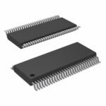 74ALVCH162836VRE4
The activity of extra discounts on wholesale prices is in full swing…
Please fill in your contact information and we will send you the latest wholesale price list.





