 ChipApex | Global Electronic Components Supplier
SEARCH
Search Product
Search Post
— IC芯片 | 连接器 | 传感器 | 被动器件 —
Search productSearch post
— IC芯片 | 连接器 | 传感器 | 被动器件 —
Consult the customer manager about the wholesale price.
consultation hotline:86-132-6715-2157
email:[email protected]
Contact the product manager for consultation. One-stop consultation is available.
Do you want a lower wholesale price? Please send us your inquiry and we will reply immediately.
The Nexperia 74ALVCH16500DGGY is an 18-bit universal bus transceiver with 3-state outputs, housed in a TSSOP56 (SOT364-1) package. It supports a supply voltage range of 1.65 V to 3.6 V and operates within an ambient temperature range of -40 °C to +85 °C. The device features bus hold inputs, low power CMOS dissipation, and IOFF circuitry for partial power-down applications. It provides direct interface with TTL levels at 2.7 V to 3.6 V and includes multiple VCC and GND pins to minimize noise and ground bounce.
Verify the specific ordering suffix 'Y' against the manufacturer's official documentation to confirm packaging details such as reel or cut tape specifications. Confirm that the TSSOP56 package variant matches the required board layout dimensions. Ensure compliance with moisture sensitivity level requirements during assembly processing.
Select this component when an 18-bit width is required for universal bus applications. The inclusion of latch enables allows for data storage directly within the transceiver, reducing external logic complexity. Verify that the operating voltage aligns with the 1.65 V to 3.6 V range and that the thermal performance meets the -40 °C to +85 °C specification.
This device belongs to the ALVCH logic family, characterized by advanced low-voltage CMOS technology. It is part of Nexperia's portfolio of universal bus transceivers designed for high-speed data transfer. The product utilizes a standard MULTIBYTE flow-through pin-out architecture, ensuring compatibility with existing designs while offering enhanced performance through reduced inductance.
Consult the official datasheet for cross-reference information. No specific substitute part numbers are documented in the provided source material.
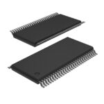 74ALVCH16500DGGY
The activity of extra discounts on wholesale prices is in full swing…
Please fill in your contact information and we will send you the latest wholesale price list.





