 ChipApex | Global Electronic Components Supplier
SEARCH
Search Product
Search Post
— IC芯片 | 连接器 | 传感器 | 被动器件 —
Search productSearch post
— IC芯片 | 连接器 | 传感器 | 被动器件 —
Consult the customer manager about the wholesale price.
consultation hotline:86-132-6715-2157
email:[email protected]
Contact the product manager for consultation. One-stop consultation is available.
Do you want a lower wholesale price? Please send us your inquiry and we will reply immediately.
The Nexperia 74ALVCH16600DGG:11 is an 18-bit universal bus transceiver with 3-state outputs, housed in a TSSOP56 (SOT364-1) package. It operates within a supply voltage range of 1.65 V to 3.6 V and supports ambient temperatures from -40 °C to +85 °C. Propagation delay ranges from 1.0 ns to 5.7 ns depending on voltage conditions. The device provides ±24 mA current drive at 3.0 V and includes bus hold inputs for data retention.
Verify the specific ordering suffix :11 against the manufacturer's latest documentation to confirm packaging details. Confirm that the TSSOP56 variant meets thermal requirements for the intended operating environment. Ensure design compatibility with the specified 1.65 V to 3.6 V supply range before finalizing procurement.
Select this component when an 18-bit width is required alongside integrated latching functionality. The MULTIBYTE™ architecture simplifies routing compared to discrete solutions. Verify that the control signals align with the active LOW/OH logic states defined in the functional description table.
This device belongs to the ALVCH logic family, utilizing Advanced Low-Voltage CMOS High-speed technology. It serves as a bridge between different voltage domains while providing storage capabilities via its internal flip-flops/latches, distinguishing it from standard non-latched transceivers.
Direct substitutes include other 18-bit universal bus transceivers with identical pinouts and latching features. Verify package compatibility (TSSOP56) and electrical specifications such as propagation delay and drive current before substitution.
The device utilizes IOFF circuitry which disables the outputs when powered down, effectively preventing potentially damaging backflow current through the device.
Data flow direction is managed independently for each path using separate output enable (OEAB/OEBA), latch enable (LEAB/LEBA), clock enable (CEAB/CEBA), and clock (CPAB/CPBA) inputs.
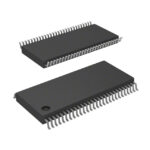 74ALVCH16600DGG:11
The activity of extra discounts on wholesale prices is in full swing…
Please fill in your contact information and we will send you the latest wholesale price list.





