 ChipApex | Global Electronic Components Supplier
SEARCH
Search Product
Search Post
— IC芯片 | 连接器 | 传感器 | 被动器件 —
Search productSearch post
— IC芯片 | 连接器 | 传感器 | 被动器件 —
Consult the customer manager about the wholesale price.
consultation hotline:86-132-6715-2157
email:[email protected]
Contact the product manager for consultation. One-stop consultation is available.
Do you want a lower wholesale price? Please send us your inquiry and we will reply immediately.
The 74ALVCH16601DGG112 is an 18-bit universal bus transceiver with 3-state outputs, manufactured by Nexperia. It operates within a supply voltage range of 1.65 V to 3.6 V and supports data flow in both directions controlled by output enable, latch enable, clock enable, and clock inputs. The device features bus hold inputs, low power CMOS dissipation, and direct interface with TTL levels. It includes IOFF circuitry for partial power-down applications and complies with JEDEC standards for various voltage ranges.
Verify the specific ordering suffix '112' against official Nexperia documentation to confirm reel size or tape width specifications. Ensure the procurement channel sources genuine Nexperia products to guarantee compliance with the specified electrical characteristics and package dimensions. Cross-reference the part number with the latest product status information available on the manufacturer's website.
Select this component when an 18-bit wide bidirectional interface is required with latching capability. It is suitable for systems operating at supply voltages between 1.65 V and 3.6 V. Consider its bus hold feature if external pull-ups are undesirable. Verify that the TSSOP56 package fits the PCB layout constraints and thermal requirements of the design.
This device belongs to the ALVCH logic family, characterized by high-speed operation and compatibility with 3.3 V systems while accepting 5 V tolerant inputs. It serves as a registered bus transceiver, offering storage capability alongside transmission functions. The DGG variant indicates a plastic thin shrink small outline package with 56 leads, designed for surface-mount assembly.
The 74ALVCH16601DGG is the base part number; verify if the '112' suffix denotes a specific packaging variation rather than a functional change. Direct pin-to-pin replacements must maintain the 18-bit width and 3-state output configuration. Check for updated revisions in the Nexperia portfolio to ensure availability and parameter consistency.
Data flow is controlled independently for A-to-B and B-to-A directions using separate output enable (OE), latch enable (LE), clock enable (CE), and clock (CP) inputs.
Bus hold inputs maintain the last state of the data line, eliminating the need for external pull-up or pull-down resistors and preventing floating inputs.
Yes, it includes IOFF circuitry that automatically disables the outputs to prevent potentially damaging backflow current when the device is powered down.
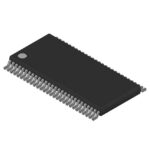 74ALVCH16601DGG112
The activity of extra discounts on wholesale prices is in full swing…
Please fill in your contact information and we will send you the latest wholesale price list.





