 ChipApex | Global Electronic Components Supplier
74ALVCH16821DGGS
Search Product
Search Post
— IC芯片 | 连接器 | 传感器 | 被动器件 —
Search productSearch post
— IC芯片 | 连接器 | 传感器 | 被动器件 —
Consult the customer manager about the wholesale price.
consultation hotline:86-132-6715-2157
email:[email protected]
Contact the product manager for consultation. One-stop consultation is available.
Do you want a lower wholesale price? Please send us your inquiry and we will reply immediately.
The 74ALVCH16821DGGS is a 20-bit bus-interface D-type flip-flop manufactured by Nexperia. It features positive-edge triggering and 3-State outputs, designed for high-speed data storage applications. The device operates within a supply voltage range of 2.3 V to 3.6 V, supporting both 2.3 V–2.7 V and 3.0 V–3.6 V logic levels. It exhibits a maximum propagation delay of 4.5 ns at 3.3 V with a 50 pF load. The component is housed in a 56-BSSOP package (7.50 mm wide) and functions within an operating temperature range of -40 °C to +85 °C.
Verify the specific suffix 'DGGS' against the manufacturer's official documentation to confirm the exact tape-and-reel packaging configuration and moisture sensitivity level. Ensure that the requested quantity aligns with standard factory reel sizes to avoid partial reel handling issues. Confirm RoHS compliance status directly from the latest datasheet revision before finalizing procurement orders.
Select this component when designing systems requiring 20-bit synchronous data storage with low propagation delay. It is suitable for interfaces demanding 3-State output control to manage bus contention. Consider the 56-pin BSSOP package constraints for PCB layout density. Verify that the system power supply remains stable within the 2.3 V to 3.6 V operational window to ensure timing integrity.
This part belongs to the 74ALVCH series of advanced low-voltage CMOS logic devices. The series is characterized by high switching speeds and compatibility with various logic families. The 74ALVCH16821 specifically addresses the need for wide-bus data latching in modern electronic equipment, offering a balance between speed and power consumption for portable and industrial applications.
Publicly confirmed substitute part numbers are not available in the provided source material.
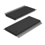 74ALVCH16821DGGS
The activity of extra discounts on wholesale prices is in full swing…
Please fill in your contact information and we will send you the latest wholesale price list.





