 ChipApex | Global Electronic Components Supplier

SEARCH
Search Product
Search Post
— IC芯片 | 连接器 | 传感器 | 被动器件 —
Search productSearch post
— IC芯片 | 连接器 | 传感器 | 被动器件 —
Consult the customer manager about the wholesale price.
consultation hotline:86-132-6715-2157
email:[email protected]
Contact the product manager for consultation. One-stop consultation is available.
Do you want a lower wholesale price? Please send us your inquiry and we will reply immediately.
The Nexperia 74ALVCH16841DGG:11 is a 20-bit bus interface D-type latch featuring two independent 10-bit registers with 3-state outputs. It operates within a supply voltage range of 2.3 V to 3.6 V, supporting propagation delays as low as 2.4 ns at 3.3 V. The device provides ±24 mA output drive capability and includes active bus hold circuitry on all data inputs. It is housed in a TSSOP56 (SOT364-1) package and complies with JEDEC standards for 2.3 V to 3.6 V operation.
Verify the specific ordering suffix :11 against current Nexperia documentation to confirm package variant and tape-and-reel specifications. Confirm RoHS compliance status directly with the manufacturer, as regulatory requirements may change. Ensure the procurement channel sources from authorized distributors to guarantee component authenticity and traceability.
Select this component when designing systems requiring 20-bit parallel data latching with high-speed performance. The ALVCH series is appropriate for applications needing direct TTL level interfacing and low power consumption. Verify that the operating temperature range of -40 °C to +85 °C meets the environmental requirements of the target application.
This part belongs to the Nexperia 74ALVCH family of advanced low-voltage CMOS logic devices. The 74ALVCH16841 specifically addresses the need for wide-bus data storage in modern electronic systems. It serves as a bridge between processor buses and peripheral devices, ensuring data integrity during transfer operations.
Check for updated versions of the 74ALVCH16841 series. Consult Nexperia's official replacement guide for any pin-compatible alternatives if this specific package version is discontinued.
The active bus hold circuitry holds unused or floating data inputs at a valid logic level, eliminating the need for external pull-up or pull-down resistors.
When nOE is HIGH, the outputs enter a high-impedance OFF state. This operation does not affect the internal state of the flip-flops.
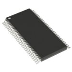 74ALVCH16841DGG:11

The activity of extra discounts on wholesale prices is in full swing…
Please fill in your contact information and we will send you the latest wholesale price list.





