 ChipApex | Global Electronic Components Supplier
SEARCH
Search Product
Search Post
— IC芯片 | 连接器 | 传感器 | 被动器件 —
Search productSearch post
— IC芯片 | 连接器 | 传感器 | 被动器件 —
Consult the customer manager about the wholesale price.
consultation hotline:86-132-6715-2157
email:[email protected]
Contact the product manager for consultation. One-stop consultation is available.
Do you want a lower wholesale price? Please send us your inquiry and we will reply immediately.
The SN74ALVCH16903DGGRG4 is a 3.3-V, 12-bit universal bus driver with parity checker and dual 3-state outputs. It operates within a supply voltage range of 2.3 V to 3.6 V. The device supports clock frequencies up to 125 MHz. Propagation delays are specified between 1.1 ns and 6.5 ns depending on the mode and voltage. Output drive capabilities include -24 mA high-level and 24 mA low-level currents at 3 V. It features active bus-hold circuitry and ESD protection exceeding 2000 V per MIL-STD-883. Operating temperature ranges from 0 °C to 70 °C.
Verify the specific ordering suffix matches the required package type and environmental rating. Confirm RoHS compliance status and moisture sensitivity level requirements against your manufacturing process specifications. Ensure the operating temperature range aligns with your system's thermal environment constraints before finalizing procurement.
Select this component when designing 3.3-V logic interfaces requiring both buffering and latching capabilities. Consider its parity checking feature if data integrity verification is necessary within the bus architecture. Evaluate the propagation delay characteristics against your maximum clock frequency requirements to ensure signal timing margins are met across the full operating voltage range.
This device belongs to Texas Instruments' Widebus family, designed for high-density bus applications. It utilizes EPIC submicron CMOS technology to achieve enhanced performance. The DGGRG4 designation indicates a Thin Shrink Small-Outline (DGG) package variant manufactured under specific quality and environmental standards defined by the manufacturer.
Public confirmed substitute part numbers: SN74ALVCH16903DLR, SN74ALVCH16903DL.
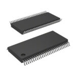 74ALVCH16903DGGRG4
The activity of extra discounts on wholesale prices is in full swing…
Please fill in your contact information and we will send you the latest wholesale price list.






