 ChipApex | Global Electronic Components Supplier

SEARCH
Search Product
Search Post
— IC芯片 | 连接器 | 传感器 | 被动器件 —
Search productSearch post
— IC芯片 | 连接器 | 传感器 | 被动器件 —
Consult the customer manager about the wholesale price.
consultation hotline:86-132-6715-2157
email:[email protected]
Contact the product manager for consultation. One-stop consultation is available.
Do you want a lower wholesale price? Please send us your inquiry and we will reply immediately.
The 74ALVT16260DL,512 is a 12-bit to 24-bit multiplexed D-type latch manufactured by NXP USA Inc. It operates at VCC supply voltages of 2.3 V to 2.7 V or 3.0 V to 3.6 V. The device features three 12-bit I/O ports (A, 1B, and 2B) for address or data transfer. Propagation delays range from 0.7 ns to 5.6 ns depending on the signal path and voltage. Output drive capability reaches +64 mA and -32 mA. It includes bus hold inputs, power-up reset, and ESD protection exceeding 2000 V per MIL STD 883C.
Verify the specific package variant required, as the DL suffix denotes SSOP56 while DGG denotes TSSOP56. Confirm that the design accounts for the active LOW output enable inputs and the necessity of tying these inputs to VCC via pull-up resistors to ensure the high-impedance state during power transitions. Ensure compatibility with the specified 5 V I/O levels.
Select this component when designing systems that require flexible routing between multiple 12-bit data sources and a common bus. The device is suitable for environments needing robust ESD protection and bus hold capabilities without external components. Consider the propagation delay specifications relative to system clock speeds and verify that the 56-pin SSOP or TSSOP footprint fits the PCB layout constraints.
This device belongs to the ALVT logic family, characterized by BiCMOS technology offering low static and dynamic power dissipation combined with high-speed operation. It is designed for 2.5 V and 3.3 V operation with 5 V tolerant I/O. The 74ALVT16260 specifically addresses complex data routing needs within this family by providing multiplexed latching functions.
The 74ALVT16260DGG is a direct pin-compatible alternative available in a TSSOP56 package instead of the standard SSOP56.
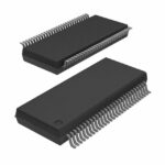 74ALVT16260DL,512

The activity of extra discounts on wholesale prices is in full swing…
Please fill in your contact information and we will send you the latest wholesale price list.





