 ChipApex | Global Electronic Components Supplier
SEARCH
Search Product
Search Post
— IC芯片 | 连接器 | 传感器 | 被动器件 —
Search productSearch post
— IC芯片 | 连接器 | 传感器 | 被动器件 —
Consult the customer manager about the wholesale price.
consultation hotline:86-132-6715-2157
email:[email protected]
Contact the product manager for consultation. One-stop consultation is available.
Do you want a lower wholesale price? Please send us your inquiry and we will reply immediately.
The Nexperia 74AUP1G0832GS,132 is a low-power 3-input AND-OR gate in the 74AUP series. It operates on a supply voltage range of 0.8 V to 3.6 V and features Schmitt-trigger inputs for noise tolerance. The device includes IOFF circuitry for partial power-down mode operation, preventing backflow current. It complies with JEDEC standards JESD8-12 through JESD8-B. ESD protection exceeds 5000 V (HBM) and 1000 V (CDM). The component is specified for ambient temperatures from -40 °C to +125 °C.
Verify the specific suffix GS,132 corresponds to the XSON6 SOT1202 package when ordering. Confirm that the application environment remains within the recommended operating conditions of 0.8 V to 3.6 V supply voltage and -40 °C to +125 °C temperature range. Ensure design safeguards are implemented to handle stress above limiting values, as permanent damage may occur if absolute maximum ratings are exceeded.
Select this component when a single gate performing an AND-OR logic function is required in a space-constrained design. The XSON6 package offers a leadless solution suitable for surface-mount applications. Consider the low static power consumption and wide supply voltage range for battery-operated or portable devices. Verify that the propagation delay characteristics meet the timing requirements of the target system under the intended load capacitance.
This part belongs to the 74AUP family of advanced ultra-low power CMOS logic devices. The 74AUP1G0832 specifically implements a 3-input AND-OR gate structure. It is distinct from standard NAND or OR gates by combining both logic operations in a single package. The GS variant utilizes the SOT1202 leadless package format, differentiating it from TSSOP or other XSON versions within the same logical family.
Direct pin-to-pin replacements must maintain the 3-input AND-OR functionality and compatible supply voltage range. Verify that alternative components support the required Schmitt-trigger input characteristics and IOFF power-down behavior. Package dimensions for the SOT1202 form factor must be checked against any substitute parts to ensure mechanical fit.
The IOFF circuitry disables the output when the device is powered down, preventing potentially damaging backflow current through the device even if input or output voltages are between 0 V and 3.6 V while VCC is 0 V.
The device implements the logic function Y = (A × B) + C, where A and B are inputs to an AND gate, and their result is combined with input C via an OR gate to produce output Y.
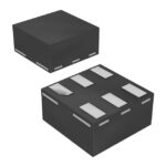 74AUP1G0832GS,132
The activity of extra discounts on wholesale prices is in full swing…
Please fill in your contact information and we will send you the latest wholesale price list.





