 ChipApex | Global Electronic Components Supplier

SEARCH
Search Product
Search Post
— IC芯片 | 连接器 | 传感器 | 被动器件 —
Search productSearch post
— IC芯片 | 连接器 | 传感器 | 被动器件 —
Consult the customer manager about the wholesale price.
consultation hotline:86-132-6715-2157
email:[email protected]
Contact the product manager for consultation. One-stop consultation is available.
Do you want a lower wholesale price? Please send us your inquiry and we will reply immediately.
74AUP1G126FW4-7 is listed in the Buffers, Drivers, Receivers, Transceivers range at ChipApex. The manufacturer field lists Diodes Incorporated. Its product description is IC BUFFER NON-INVERT 3.6V 6DFN. Review the specifications below when checking this part for your BOM.
The 74AUP1G126FW4-7 is a single non-inverting buffer with three-state output from the Advanced Ultra Low Power (AUP) CMOS logic family. It operates within a supply voltage range of 0.8V to 3.6V and features Schmitt trigger inputs for noise tolerance. The device provides ±4mA output drive at 3.0V and includes I_OFF circuitry to prevent backflow current during partial power-down modes. It is housed in an X2-DFN1010-6 package.
Verify the specific ordering suffix FW4 corresponds to the X2-DFN1010-6 package configuration before procurement. Confirm that the -7 suffix indicates the standard 5,000-unit tape and reel packing quantity. Ensure compatibility with the required operating temperature range of -40°C to +125°C for the intended application environment.
Select this component for portable applications requiring low static power consumption and wide supply voltage flexibility. The inclusion of Schmitt triggers makes it suitable for environments with noisy signals or slow input transitions. Verify that the single-channel architecture meets the system's buffering requirements without unnecessary channel utilization.
This part belongs to the 74AUP1G126 series of single-buffer gates manufactured by Diodes Incorporated. It utilizes the AUP logic family, which is optimized for ultra-low power dissipation across the entire voltage range. The device is fully lead-free, RoHS compliant, and halogen/antimony free, adhering to environmental standards.
Cross-reference with other packages in the same series such as 74AUP1G126SE-7 (SOT353), 74AUP1G126FS3-7 (X2-DFN0808-4), or 74AUP1G126FX4-7 (X2-DFN1409-6). Ensure pinout compatibility and thermal resistance characteristics match the PCB layout constraints when substituting package types.
The device features I_OFF circuitry that disables the output, preventing damaging backflow current through the device when it is powered down.
The Output Enable (OE) pin controls the three-state output. When a LOW-level signal is applied to OE, the output enters a high-impedance state.
Explore related parts through Logic, Integrated Circuits (ICs), all product categories, ChipApex homepage.
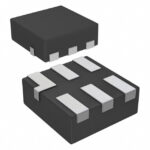 74AUP1G126FW4-7

The activity of extra discounts on wholesale prices is in full swing…
Please fill in your contact information and we will send you the latest wholesale price list.





