 ChipApex | Global Electronic Components Supplier

SEARCH
Search Product
Search Post
— IC芯片 | 连接器 | 传感器 | 被动器件 —
Search productSearch post
— IC芯片 | 连接器 | 传感器 | 被动器件 —
Consult the customer manager about the wholesale price.
consultation hotline:86-132-6715-2157
email:[email protected]
Contact the product manager for consultation. One-stop consultation is available.
Do you want a lower wholesale price? Please send us your inquiry and we will reply immediately.
The Nexperia 74AUP1G19GW,125 is a low-power 1-of-2 decoder/demultiplexer housed in a TSSOP6 (SOT363-2) package. It features a common enable input and provides true and complement outputs. The device operates across a wide supply voltage range of 0.8 V to 3.6 V with Schmitt-trigger inputs for noise immunity. Static power consumption is specified at a maximum of 0.9 µA within the -40 °C to +125 °C temperature range.
Verify the specific ordering suffix matches the required package type, as the AUP1G19 series is available in multiple configurations including XSON variants. Confirm that the TSSOP6 designation aligns with your board layout requirements. Ensure the selected component meets the necessary environmental specifications for your intended operating temperature range before finalizing procurement.
Select this component for designs requiring a single-channel decoder with complementary outputs in a minimal footprint. The wide voltage compatibility supports mixed-voltage interfaces without external level shifting. Consider the propagation delay characteristics relative to your system clock speed and load capacitance to ensure signal integrity is maintained under dynamic operating conditions.
This part belongs to the Nexperia 74AUP family of ultra-low-power CMOS logic devices. The AUP series is designed for battery-powered applications due to its extended voltage range and reduced static current consumption compared to standard logic families. The 1G prefix indicates a single functional circuit contained within a compact surface-mount package suitable for high-density PCB assembly.
Direct pin-compatible replacements include other 74AUP1G19 variants such as the GM or GN versions if different package footprints are acceptable. Verify that any substitute maintains the same TSSOP6 outline dimensions and electrical characteristics, particularly the IOFF functionality and Schmitt-trigger thresholds.
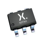 74AUP1G19GW,125

The activity of extra discounts on wholesale prices is in full swing…
Please fill in your contact information and we will send you the latest wholesale price list.






