 ChipApex | Global Electronic Components Supplier
SEARCH
Search Product
Search Post
— IC芯片 | 连接器 | 传感器 | 被动器件 —
Search productSearch post
— IC芯片 | 连接器 | 传感器 | 被动器件 —
Consult the customer manager about the wholesale price.
consultation hotline:86-132-6715-2157
email:[email protected]
Contact the product manager for consultation. One-stop consultation is available.
Do you want a lower wholesale price? Please send us your inquiry and we will reply immediately.
The Nexperia 74AUP1G885GF,115 is a low-power dual function gate housed in an 8-XSON (SOT1203) package. It features three inputs (A, B, C) and two outputs (1Y, 2Y). Output 1Y implements the Boolean function A × C, while output 2Y implements A × B + A × C. The device operates on a supply voltage range of 0.8 V to 3.6 V with a maximum static supply current of 0.9 µA at -40 °C to +85 °C. Propagation delay ranges from 2.1 ns to 4.2 ns depending on load capacitance and temperature.
Verify the specific suffix GF corresponds to the SOT1203 XSON8 package variant. Confirm the component status as End-of-Life (EOL) based on manufacturer notices. Ensure design-in validation accounts for the specified operating temperature range and electrical characteristics prior to final procurement decisions.
Select this component when a single IC must provide two distinct dual-function logic operations within a minimal footprint. The choice is driven by the requirement for low static power consumption across a wide voltage range and the need for robust input signal conditioning via Schmitt triggers.
This part belongs to the 74AUP series of ultra-low-power CMOS logic devices manufactured by Nexperia. It is designed for portable and battery-operated applications where minimizing power dissipation is critical. The device utilizes advanced semiconductor processes to achieve high performance at low voltages.
The 74AUP1G885GS,115 is listed as a manufacturer-recommended alternative. Verify pinout compatibility and package dimensions before substitution.
Output 1Y performs the AND operation A × C. Output 2Y performs the function A × B + A × C.
The IOFF circuitry disables the outputs when the device is powered down, preventing potentially damaging backflow current through the device.
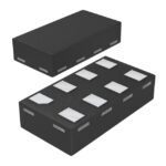 74AUP1G885GF,115
The activity of extra discounts on wholesale prices is in full swing…
Please fill in your contact information and we will send you the latest wholesale price list.





