 ChipApex | Global Electronic Components Supplier

SEARCH
Search Product
Search Post
— IC芯片 | 连接器 | 传感器 | 被动器件 —
Search productSearch post
— IC芯片 | 连接器 | 传感器 | 被动器件 —
Consult the customer manager about the wholesale price.
consultation hotline:86-132-6715-2157
email:[email protected]
Contact the product manager for consultation. One-stop consultation is available.
Do you want a lower wholesale price? Please send us your inquiry and we will reply immediately.
The 74AUP1G97FW4-7 is a single configurable multiple-function gate from Diodes Incorporated, utilizing Advanced Ultra Low-Power (AUP) CMOS technology. It features three data inputs and one push-pull output housed in an X2-DFN1010-6 package. The device operates within a supply voltage range of 0.8V to 3.6V. It supports logic functions including MUX, AND, OR, NAND, NOR, inverter, and non-inverting buffer via 3-bit input patterns. Key electrical characteristics include ±4mA output drive at 3.0V, low static power consumption with ICC less than 0.9µA, and typical power dissipation capacitance of 4.8pF at 3.6V.
Verify the component matches the exact manufacturer part number 74AUP1G97FW4-7 from Diodes Incorporated. Confirm the package type is X2-DFN1010-6 and that it complies with RoHS directives. Ensure the supplier provides valid traceability documentation. Check for any specific handling requirements related to ESD protection during storage and assembly.
Select this component when a single gate needs to perform various logic functions dynamically without changing hardware. It is suitable for mixed-voltage environments due to 3.6V tolerant inputs. Consider its low power profile for battery-operated devices. Verify that the required logic functions align with the available configuration patterns defined in the datasheet.
This part belongs to the 74AUP1G series of single-gate logic devices. It is part of the AUP family designed for low-voltage applications ranging from 0.8V to 3.6V. The FW4 suffix indicates the X2-DFN1010-6 leadless package. It serves as a versatile alternative to fixed-function gates in space-constrained designs.
Direct substitutes include other 74AUP1G97 variants from different manufacturers or packages, such as those in SOT26 or SOT363, provided pin compatibility and electrical specifications match. Cross-referencing with Nexperia or ON Semiconductor equivalents may be necessary if sourcing constraints exist.
The logic function is determined by eight patterns of 3-bit input applied to pins A, B, and C. Users can select functions like MUX, AND, OR, NAND, NOR, inverter, or buffer based on these input states.
The IOFF circuitry supports partial-power-down mode operation by disabling the output. This prevents potentially damaging backflow current through the device when it is powered down while other parts of the system remain active.
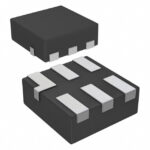 74AUP1G97FW4-7

The activity of extra discounts on wholesale prices is in full swing…
Please fill in your contact information and we will send you the latest wholesale price list.





