 ChipApex | Global Electronic Components Supplier

SEARCH
Search Product
Search Post
— IC芯片 | 连接器 | 传感器 | 被动器件 —
Search productSearch post
— IC芯片 | 连接器 | 传感器 | 被动器件 —
Consult the customer manager about the wholesale price.
consultation hotline:86-132-6715-2157
email:[email protected]
Contact the product manager for consultation. One-stop consultation is available.
Do you want a lower wholesale price? Please send us your inquiry and we will reply immediately.
The Nexperia 74AUP1G98GW,125 is a low-power configurable multiple function gate housed in a TSSOP6 (SOT363-2) package. It operates on a supply voltage range of 0.8 V to 3.6 V with Schmitt-trigger inputs. The device supports logic functions including MUX, AND, OR, NAND, NOR, inverter, and buffer via a 3-bit input configuration. Static power consumption is maximized at 0.9 μA. Propagation delay ranges from 1.6 ns to 5.8 ns depending on load capacitance and voltage. Operating temperature spans -40 °C to +125 °C.
Verify the specific ordering suffix matches the required package variant. Confirm that the component status remains active before finalizing design-in decisions. Ensure compliance with JEDEC standards relevant to the target operating voltage range. Validate thermal dissipation requirements against ambient temperature conditions during system integration.
Select this component when a single gate must perform multiple logic roles within space-constrained designs. The wide supply voltage range accommodates various low-power logic families. Verify that the TSSOP6 footprint aligns with existing PCB layout constraints. Consider the propagation delay specifications relative to the maximum switching frequency of the application.
This part belongs to the 74AUP series of ultra-low-power CMOS logic devices. It shares functional similarities with other configurable gates but offers specific Schmitt-trigger characteristics. The GW suffix denotes the TSSOP6 plastic thin shrink small outline package. It serves as a versatile alternative to discrete logic implementations in compact electronic assemblies.
Direct substitutes include other 74AUP1G98 variants such as 74AUP1G98GM or 74AUP1G98GN, provided the package type difference is acceptable for the mechanical design.
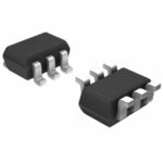 74AUP1G98GW,125

The activity of extra discounts on wholesale prices is in full swing…
Please fill in your contact information and we will send you the latest wholesale price list.





