 ChipApex | Global Electronic Components Supplier
74AUP1GU04GW,125
Search Product
Search Post
— IC芯片 | 连接器 | 传感器 | 被动器件 —
Search productSearch post
— IC芯片 | 连接器 | 传感器 | 被动器件 —
Consult the customer manager about the wholesale price.
consultation hotline:86-132-6715-2157
email:[email protected]
Contact the product manager for consultation. One-stop consultation is available.
Do you want a lower wholesale price? Please send us your inquiry and we will reply immediately.
The Nexperia 74AUP1GU04GW,125 is a single unbuffered inverter housed in a TSSOP5 (SOT353-1) package. It operates within a supply voltage range of 0.8 V to 3.6 V and supports an ambient temperature range from -40 °C to +125 °C. The device features low static power consumption with a maximum ICC of 0.9 μA at extended temperatures. Propagation delay ranges from 0.3 ns to 5.7 ns depending on load capacitance and voltage. Input leakage current is specified at ±0.75 μA maximum under full temperature conditions.
Verify the specific suffix 'GW' corresponds to the TSSOP5 plastic thin shrink small outline package with a body width of 1.25 mm. Confirm that the required temperature grade matches the -40 °C to +125 °C specification listed for this variant. Ensure input and output current limits are respected to prevent exceeding absolute maximum ratings during design integration.
Select this component when a single inverting function is required in a minimal footprint surface-mount configuration. The wide supply voltage compatibility allows direct interfacing with various logic families operating between 0.8 V and 3.6 V. Consider the low propagation delay characteristics for high-speed signal inversion applications where power efficiency is a primary constraint.
This device belongs to the 74AUP1Gxx series of ultra-low-power CMOS logic gates manufactured by Nexperia. The AUP family is designed for applications requiring reduced power dissipation while maintaining high-speed performance. The GW suffix specifically denotes the TSSOP5 package option within this broader portfolio of single-gate logic solutions.
Consult official Nexperia documentation for verified substitute part numbers. Cross-referencing should prioritize devices with identical logical functions, compatible supply voltage ranges, and matching package dimensions to ensure mechanical and electrical interchangeability without redesign.
Yes, the device includes IOFF circuitry that enables partial power-down mode operation to minimize current consumption when the system is not active.
The inputs are overvoltage tolerant up to 3.6 V, allowing them to handle signals higher than the supply voltage without damage, provided current limits are observed.
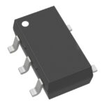 74AUP1GU04GW,125
The activity of extra discounts on wholesale prices is in full swing…
Please fill in your contact information and we will send you the latest wholesale price list.




