 ChipApex | Global Electronic Components Supplier

SEARCH
Search Product
Search Post
— IC芯片 | 连接器 | 传感器 | 被动器件 —
Search productSearch post
— IC芯片 | 连接器 | 传感器 | 被动器件 —
Consult the customer manager about the wholesale price.
consultation hotline:86-132-6715-2157
email:[email protected]
Contact the product manager for consultation. One-stop consultation is available.
Do you want a lower wholesale price? Please send us your inquiry and we will reply immediately.
The Nexperia 74AUP1T98GW,125 is a low-power configurable gate with voltage-level translator housed in a 6-TSSOP package. It operates on a supply voltage (VCC) of 2.3 V to 3.6 V and supports an ambient temperature range from -40 °C to +125 °C. The device features Schmitt-trigger inputs and IOFF circuitry for partial power-down applications. It provides unidirectional level translation between A-side logic levels (1.8 V to 2.7 V) and B-side logic levels (2.3 V to 3.6 V).
Verify the complete part number including the ordering suffix
Select this component when a single IC must perform multiple logic functions while simultaneously translating signal voltages between two distinct domains. Ensure the application requires unidirectional data flow from the A-side inputs to the B-side output. Confirm that the system voltage ranges align with the specified VCCA and VCCB limits to maintain proper logic threshold performance.
This device belongs to the Nexperia 74AUP series, which utilizes advanced CMOS technology for low power consumption and high-speed operation. The 74AUP1T98 specifically combines configurable logic capabilities with integrated level shifting, distinguishing it from standard logic gates or dedicated translators. It is designed for applications requiring flexible logic implementation within strict power and size constraints.
Direct replacements require matching the 6-TSSOP package, 2.3 V to 3.6 V supply range, and configurable gate functionality with level translation. Verify pinout compatibility and ensure the substitute supports the required IOFF power-down feature if partial power-down operation is critical to the design.
The logic function is selected by connecting the three data inputs (A, B, and C) directly to VCC or GND according to the function selection table provided in the datasheet.
The IOFF circuitry disables the output when the device is powered down (VCC = 0 V), preventing damaging backflow current through the device when connected to live buses.
No, the 74AUP1T98 is a unidirectional device. Data flows from the A-side inputs (configured for lower voltage levels) to the B-side output (compatible with higher voltage levels).
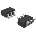 74AUP1T98GW,125

The activity of extra discounts on wholesale prices is in full swing…
Please fill in your contact information and we will send you the latest wholesale price list.





