 ChipApex | Global Electronic Components Supplier

SEARCH
Search Product
Search Post
— IC芯片 | 连接器 | 传感器 | 被动器件 —
Search productSearch post
— IC芯片 | 连接器 | 传感器 | 被动器件 —
Consult the customer manager about the wholesale price.
consultation hotline:86-132-6715-2157
email:[email protected]
Contact the product manager for consultation. One-stop consultation is available.
Do you want a lower wholesale price? Please send us your inquiry and we will reply immediately.
74AUP2G125GD,125 is listed in the Buffers, Drivers, Receivers, Transceivers range at ChipApex. The manufacturer field lists NXP USA Inc.. Its product description is IC BUFFER/LINEDVR DUAL XSON8U. Review the specifications below when checking this part for your BOM.
The NXP USA Inc. 74AUP2G125GD,125 is a low-power dual buffer and line driver featuring three-state outputs controlled by active-low enable inputs (nOE). It operates within a supply voltage range of 0.8 V to 3.6 V and includes Schmitt-trigger inputs for noise immunity. The device incorporates IOFF circuitry to prevent backflow current during partial power-down states. It supports an ambient operating temperature from -40 °C to +125 °C and complies with JEDEC standards JESD8-12 through JESD8-B.
Verify the specific package designation GD corresponds to the required footprint and thermal characteristics. Confirm the ordering suffix matches the intended temperature grade and manufacturing revision. Ensure compatibility with existing board layouts regarding pin assignments and electrical tolerances before finalizing procurement.
Select this component for designs requiring dual non-inverting buffers with three-state control in ultra-low voltage applications. The inclusion of Schmitt triggers makes it suitable for noisy environments or signals with gradual transitions. Verify that the required output drive capability and propagation delay meet the system timing constraints under the target load conditions.
This part belongs to the Nexperia 74AUP series of advanced ultra-low power CMOS logic devices. The series is designed for portable and battery-operated applications where minimizing power consumption is critical while maintaining signal integrity across wide voltage ranges.
The datasheet revision history indicates that type number 74AUP2G125GD was removed in version 12. Verify if alternative packages such as DC, GT, GN, GS, or GX are available substitutes for the same functional specification.
The device utilizes IOFF circuitry which automatically disables the outputs to prevent potentially damaging backflow current through the device when it is powered down.
The Schmitt-trigger action at all inputs makes the circuit tolerant of slower input rise and fall times, improving noise immunity.
Explore related parts through Logic, Integrated Circuits (ICs), all product categories, ChipApex homepage.
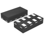 74AUP2G125GD,125

The activity of extra discounts on wholesale prices is in full swing…
Please fill in your contact information and we will send you the latest wholesale price list.





