 ChipApex | Global Electronic Components Supplier

SEARCH
Search Product
Search Post
— IC芯片 | 连接器 | 传感器 | 被动器件 —
Search productSearch post
— IC芯片 | 连接器 | 传感器 | 被动器件 —
Consult the customer manager about the wholesale price.
consultation hotline:86-132-6715-2157
email:[email protected]
Contact the product manager for consultation. One-stop consultation is available.
Do you want a lower wholesale price? Please send us your inquiry and we will reply immediately.
The Nexperia 74AUP2G157GN,115 is a low-power single 2-input multiplexer housed in an XSON8 package (SOT1116). It selects data from inputs I0 or I1 based on the state of the common select input S, providing true and complement outputs Y and Y. The enable input E is active LOW; when HIGH, outputs are forced to defined states. Schmitt trigger inputs ensure tolerance to slow signal transitions across the 0.8 V to 3.6 V supply range. The device supports partial power-down via IOFF circuitry and operates within -40 °C to +125 °C.
Verify the ordering suffix '115' corresponds to the XSON8 SOT1116 package variant with dimensions 1.2 x 1.0 x 0.35 mm. Confirm the temperature range specification matches the required operational environment of -40 °C to +125 °C. Ensure design compatibility with the active LOW enable logic and Schmitt trigger input requirements before integration.
Select this component for designs requiring a single 2-input multiplexer with Schmitt trigger inputs to handle slow signal edges. It is suitable for applications needing partial power-down capabilities to minimize leakage current. Verify that the supply voltage remains within the 0.8 V to 3.6 V range and that the XSON8 package footprint fits the PCB layout constraints.
This part belongs to the 74AUP series of low-power CMOS logic devices manufactured by Nexperia. The AUP series is characterized by operation at low supply voltages and high speed. The 74AUP2G157 specifically denotes a dual-gate multiplexer function, offering two independent data paths controlled by a single selector line within a compact semiconductor structure.
Other variants in the 74AUP2G157 family include DC (VSSOP8), GT (XSON8 SOT833-1), and GS (XSON8 SOT1203). These share identical electrical specifications but differ in physical package dimensions and pinout orientation. Verify mechanical fit and soldering profile compatibility when substituting package types.
The IOFF circuitry disables the output drivers when the device is powered down, preventing damaging backflow current through the device if its inputs or outputs are powered while VCC is at 0 V.
When the Enable input (E) is HIGH, the true output Y is forced LOW and the complement output Y is forced HIGH, regardless of the states of the data inputs or the select input.
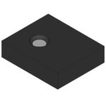 74AUP2G157GN,115

The activity of extra discounts on wholesale prices is in full swing…
Please fill in your contact information and we will send you the latest wholesale price list.





