 ChipApex | Global Electronic Components Supplier
SEARCH
Search Product
Search Post
— IC芯片 | 连接器 | 传感器 | 被动器件 —
Search productSearch post
— IC芯片 | 连接器 | 传感器 | 被动器件 —
Consult the customer manager about the wholesale price.
consultation hotline:86-132-6715-2157
email:[email protected]
Contact the product manager for consultation. One-stop consultation is available.
Do you want a lower wholesale price? Please send us your inquiry and we will reply immediately.
The Nexperia 74AUP2G3404GW,125 is a low-power buffer and inverter housed in a TSSOP6 (SOT363-2) package. It integrates one non-inverting buffer and one inverter within a single chip. The device operates across a wide supply voltage range of 0.8 V to 3.6 V. It features Schmitt trigger inputs for noise immunity and IOFF circuitry for partial power-down applications. Static supply current is specified at a maximum of 1.4 μA at -40 °C to +125 °C.
Verify the specific ordering suffix GW,125 to confirm the TSSOP6 plastic thin shrink small outline package with a body width of 1.25 mm. Ensure the temperature range requirement aligns with the -40 °C to +125 °C specification. Confirm RoHS3 compliance status if required by your manufacturing standards before finalizing procurement.
Select this component when a combined buffer and inverter function is required in a minimal footprint. The TSSOP6 package offers a compact solution for space-constrained designs. Consider the Schmitt trigger input capability if the application involves slow-rising signals or noisy environments requiring hysteresis for clean switching.
This part belongs to the 74AUP series of ultra-low-power CMOS logic devices. The AUP family is designed for applications requiring extended supply voltage ranges and low power consumption. The 74AUP2G3404 specifically combines two distinct logic functions into one package, reducing board space compared to using separate buffer and inverter components.
Check for pin-compatible alternatives such as the 74AUP2G3404GM, 74AUP2G3404GN, or 74AUP2G3404GS if different packaging options like XSON are preferred. Verify that any substitute maintains the same electrical characteristics and temperature ratings.
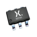 74AUP2G3404GW,125
The activity of extra discounts on wholesale prices is in full swing…
Please fill in your contact information and we will send you the latest wholesale price list.





