 ChipApex | Global Electronic Components Supplier
SEARCH
Search Product
Search Post
— IC芯片 | 连接器 | 传感器 | 被动器件 —
Search productSearch post
— IC芯片 | 连接器 | 传感器 | 被动器件 —
Consult the customer manager about the wholesale price.
consultation hotline:86-132-6715-2157
email:[email protected]
Contact the product manager for consultation. One-stop consultation is available.
Do you want a lower wholesale price? Please send us your inquiry and we will reply immediately.
The Nexperia 74AUP3G3404GSX is a low-power logic device featuring a dual buffer and a single inverter within an 8-terminal XSON package (SOT1203). It operates across a wide supply voltage range of 0.8 V to 3.6 V, ensuring high noise immunity and low static power consumption with a maximum ICC of 0.9 μA at -40 °C to +85 °C. The inputs incorporate Schmitt trigger action for tolerance to slow rise and fall times. The device includes IOFF circuitry to prevent damaging backflow currents during partial power-down applications.
Verify the specific suffix GSX corresponds to the SOT1203 XSON8 package variant when sourcing. Confirm that the required operating temperature range aligns with the specified -40 °C to +125 °C limits. Ensure design margins account for the dynamic power dissipation calculations provided in the datasheet to maintain reliability under varying load conditions.
Select this component for designs requiring mixed buffer and inverter functions in a minimal footprint. The 74AUP series offers lower power consumption compared to standard CMOS families while maintaining compatibility with voltages down to 0.8 V. Consider the XSON8 package dimensions if board space is constrained, noting the leadless construction suitable for automated surface-mount assembly.
This part belongs to the Nexperia 74AUP family of advanced ultra-low power logic devices. The 74AUP3G3404 specifically integrates three independent logic gates: two non-inverting buffers and one inverting buffer. It is designed for portable and battery-operated applications where minimizing energy usage is critical without sacrificing signal integrity or switching speed.
The 74AUP3G3404DC serves as a functional equivalent utilizing the VSSOP8 package. Designers must verify pinout compatibility and thermal performance differences between the XSON8 and VSSOP8 footprints before substitution.
The integrated IOFF circuitry disables the outputs when the device is powered down, preventing damaging backflow current from flowing through the device into the powered-down section.
The Schmitt trigger action ensures that the circuit remains tolerant of slower input rise and fall times across the entire supply voltage range, improving noise immunity.
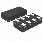 74AUP3G3404GSX
The activity of extra discounts on wholesale prices is in full swing…
Please fill in your contact information and we will send you the latest wholesale price list.




