 ChipApex | Global Electronic Components Supplier
SEARCH
Search Product
Search Post
— IC芯片 | 连接器 | 传感器 | 被动器件 —
Search productSearch post
— IC芯片 | 连接器 | 传感器 | 被动器件 —
Consult the customer manager about the wholesale price.
consultation hotline:86-132-6715-2157
email:[email protected]
Contact the product manager for consultation. One-stop consultation is available.
Do you want a lower wholesale price? Please send us your inquiry and we will reply immediately.
The Nexperia 74AVC16373DGG,512 is a 16-bit D-type transparent latch featuring separate inputs and 3-state outputs for bus-oriented applications. It consists of two independent 8-bit sections with dedicated latch enable (LE) and output enable (OE) controls per section. The device operates within a supply voltage range of 1.2 V to 3.6 V and complies with JEDEC standards JESD8-7, JESD8-5, and JESD8-1A. It incorporates Dynamic Controlled Output (DCO) circuitry to reduce noise without degrading speed. The component supports live insertion and utilizes low-inductance multiple power pins to minimize ground bounce.
Verify the specific ordering suffix against manufacturer documentation to confirm packaging details. Confirm that the requested variant matches the required temperature range and package dimensions. Ensure compatibility with JEDEC low-voltage standards relevant to the target application environment before finalizing procurement specifications.
Select this component for designs requiring fast propagation delays and low power consumption in 3.6 V tolerant environments. The dual 8-bit architecture allows flexible configuration for different data widths. Consider the DCO feature for applications sensitive to signal integrity and noise reduction on shared buses.
This part belongs to the 74AVC series of advanced very-low-voltage CMOS logic devices. It is housed in a TSSOP48 plastic thin shrink small outline package (SOT362-1). The device is manufactured by Nexperia USA Inc. and is intended for general-purpose digital logic applications operating between -40 °C and +85 °C.
Consult official Nexperia substitution guides for verified alternatives. Cross-reference pinouts and electrical characteristics carefully when considering equivalent parts from other manufacturers to ensure functional compatibility.
The DCO circuitry dynamically changes the output impedance during switching events. This reduces electromagnetic interference and noise without compromising the propagation speed of the latch.
Each 8-bit section has its own Latch Enable (LE) and Output Enable (OE) input. This allows independent control over data latching and output driving for each half of the 16-bit device.
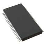 74AVC16373DGG,512
The activity of extra discounts on wholesale prices is in full swing…
Please fill in your contact information and we will send you the latest wholesale price list.





