 ChipApex | Global Electronic Components Supplier
SEARCH
Search Product
Search Post
— IC芯片 | 连接器 | 传感器 | 被动器件 —
Search productSearch post
— IC芯片 | 连接器 | 传感器 | 被动器件 —
Consult the customer manager about the wholesale price.
consultation hotline:86-132-6715-2157
email:[email protected]
Contact the product manager for consultation. One-stop consultation is available.
Do you want a lower wholesale price? Please send us your inquiry and we will reply immediately.
The 74AVC16836ADGV,112 is a 20-bit universal bus driver manufactured by Nexperia. It operates within a supply voltage range of 1.2 V to 3.6 V and features Dynamic Controlled Outputs (DCO) for noise reduction. The device utilizes a 56-pin TVSOP package with a 0.4 mm pitch. Propagation delay from input An to output Yn ranges from 0.7 ns to 5.3 ns depending on the supply voltage. Maximum clock pulse frequency reaches 500 MHz at 3.3 V.
Verify that the ordering suffix '112' corresponds to the specific tape and reel packaging configuration defined in the manufacturer's documentation. Confirm the component status as product data rather than preliminary or objective specifications. Ensure compatibility with the 56-lead TVSOP footprint SOT481-2 when designing PCB layouts.
Select this component for high-speed digital interfaces requiring registered buffering with low power consumption. The wide supply voltage range supports various logic families. The inverted register enable provides flexible control options for complex data routing architectures.
This part belongs to the 74AVC16836A family of 20-bit registered drivers. The ADGV variant specifically denotes the 56-pin plastic thin shrink small outline package with a 0.4 mm pitch. The device is designed to comply with JEDEC standards for low voltage CMOS logic.
The 74AVC16836ADGG is a compatible alternative utilizing a 56-pin TSSOP package with a 0.5 mm pitch. Verify pin-to-pin compatibility and ensure the physical footprint matches the available board space before substitution.
The Dynamic Controlled Output circuit lowers output impedance during transitions to drive loads effectively, then raises it to reduce noise, maintaining speed while improving signal integrity.
The inverted latch enable (LE) input controls the latching of data. When LE is low, data is latched on the rising edge of the clock; when high, the outputs reflect the previous state.
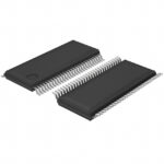 74AVC16836ADGV,112
The activity of extra discounts on wholesale prices is in full swing…
Please fill in your contact information and we will send you the latest wholesale price list.





