 ChipApex | Global Electronic Components Supplier
SEARCH
Search Product
Search Post
— IC芯片 | 连接器 | 传感器 | 被动器件 —
Search productSearch post
— IC芯片 | 连接器 | 传感器 | 被动器件 —
Consult the customer manager about the wholesale price.
consultation hotline:86-132-6715-2157
email:[email protected]
Contact the product manager for consultation. One-stop consultation is available.
Do you want a lower wholesale price? Please send us your inquiry and we will reply immediately.
The Nexperia 74AVC1T1004DPJ is a translating 1-to-4 fan-out buffer designed for clock distribution and voltage translation. It features dual independent supplies, VCC(A) and VCC(B), each ranging from 0.8 V to 3.6 V. The device accepts one data input (A) referenced to VCC(A) and provides four outputs (Yn) referenced to VCC(B). It supports maximum data rates up to 380 Mbit/s during translation between 1.8 V and 3.3 V. The component includes Schmitt trigger inputs, an active LOW output enable (OE), and IOFF circuitry to prevent backflow current during power-down. It operates within a temperature range of -40 °C to +125 °C.
Verify the package type SOT552-1 (TSSOP10) matches the design footprint. Confirm that the DPJ suffix corresponds to the specific reel or tape configuration required by assembly equipment. Ensure supply voltages remain within the 0.8 V to 3.6 V limits for both VCC(A) and VCC(B) pins to maintain JEDEC compliance.
Select this component when a single source signal must drive four distinct loads across different voltage levels. The dual-supply architecture allows flexible translation between any combination of 0.8 V, 1.2 V, 1.5 V, 1.8 V, 2.5 V, and 3.3 V. Consider the propagation delay characteristics, which vary based on the specific VCC(A) and VCC(B) settings and load capacitance, when designing high-speed timing paths.
This device belongs to the 74AVC series, characterized by Advanced Very-low-voltage CMOS technology. It is part of Nexperia's portfolio of translating buffers designed to facilitate interface connections between low-voltage components. The 1-to-4 fan-out topology distinguishes it from simple inverters or non-translating buffers, offering integrated level shifting capabilities in a compact TSSOP10 package.
The 74AVC1T1004GU is a pin-compatible alternative housed in a DHVQFN10 package. Both devices share identical electrical specifications and functionality. Verify that the target PCB layout accommodates the physical dimensions of the replacement package variant.
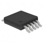 74AVC1T1004DPJ
The activity of extra discounts on wholesale prices is in full swing…
Please fill in your contact information and we will send you the latest wholesale price list.






