 ChipApex | Global Electronic Components Supplier
SEARCH
Search Product
Search Post
— IC芯片 | 连接器 | 传感器 | 被动器件 —
Search productSearch post
— IC芯片 | 连接器 | 传感器 | 被动器件 —
Consult the customer manager about the wholesale price.
consultation hotline:86-132-6715-2157
email:[email protected]
Contact the product manager for consultation. One-stop consultation is available.
Do you want a lower wholesale price? Please send us your inquiry and we will reply immediately.
The Nexperia 74AVC1T1004 is a translating 1-to-4 fan-out buffer designed for clock distribution and voltage translation. It features dual independent supplies, VCC(A) and VCC(B), each ranging from 0.8 V to 3.6 V. The device accepts one data input (A) referenced to VCC(A) and provides four outputs (Yn) referenced to VCC(B). Key electrical parameters include a maximum propagation delay of 15 ns at 3.3 V, ESD protection exceeding 2000 V (HBM) and 1000 V (CDM), and an operating temperature range of -40 °C to +125 °C. It includes Schmitt trigger inputs and IOFF circuitry for partial power-down support.
Verify the specific ordering suffix against the manufacturer's official documentation to confirm package type and tape/reel specifications. The provided datasheet references the 74AVC1T1004DP variant in TSSOP10; ensure the requested model matches the required physical footprint and handling requirements for the target assembly process.
Select this component when designing circuits that require driving multiple loads from a single source across different voltage levels. Ensure both VCC(A) and VCC(B) are within the 0.8 V to 3.6 V range. Consider the propagation delay variations based on load capacitance and supply voltage combinations when determining timing margins for high-speed applications.
This device belongs to the Nexperia AVC (Advanced Very-low-voltage CMOS) logic family, which is optimized for ultra-low power consumption and operation at very low supply voltages. The AVC series supports JEDEC standards for various voltage nodes, facilitating integration into modern portable and battery-powered electronic systems.
Public confirmed substitute part numbers: None identified in the provided source material.
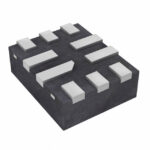 74AVC1T1004GU33Z
The activity of extra discounts on wholesale prices is in full swing…
Please fill in your contact information and we will send you the latest wholesale price list.




