 ChipApex | Global Electronic Components Supplier
SEARCH
Search Product
Search Post
— IC芯片 | 连接器 | 传感器 | 被动器件 —
Search productSearch post
— IC芯片 | 连接器 | 传感器 | 被动器件 —
Consult the customer manager about the wholesale price.
consultation hotline:86-132-6715-2157
email:[email protected]
Contact the product manager for consultation. One-stop consultation is available.
Do you want a lower wholesale price? Please send us your inquiry and we will reply immediately.
The Nexperia 74AVC1T1022GUX is a translating 1-to-4 fan-out buffer designed for clock distribution and voltage level translation. It features dual independent supplies, VCC(A) and VCC(B), each ranging from 0.8 V to 3.6 V. The device includes one data input (A), four outputs (two referenced to VCC(A) and two to VCC(B)), and an active-low output enable (OE). It supports maximum data rates up to 380 Mbit/s for translations between 1.8 V and 3.3 V. The component operates within a temperature range of -40 °C to +125 °C and utilizes Schmitt trigger inputs for noise immunity.
Verify the specific ordering suffix against the manufacturer's official documentation to confirm package type and temperature rating. The 'GU' designation corresponds to the XQFN10 package (SOT1160-1). Confirm that the required operating temperature range matches the specified -40 °C to +125 °C limit before finalizing procurement.
Select this component when a single-input, four-output buffer with simultaneous voltage translation is required. Ensure the design accommodates the dual-supply configuration, as VCC(A) and VCC(B) must be independently powered. Verify that the load capacitance requirements align with the dynamic characteristics provided in the datasheet tables for the target voltage levels.
This device belongs to the Nexperia AVC logic family, which focuses on advanced voltage translation and buffering solutions. The 74AVC1T1022 specifically addresses the need for fan-out buffers that can drive multiple loads across different voltage domains while maintaining signal integrity through Schmitt trigger action and robust ESD protection.
Direct functional replacements include other 1-to-4 translating fan-out buffers from the same family, such as the 74AVC1T1022DP (TSSOP10 package variant). Cross-family substitution requires verifying pin compatibility, supply voltage ranges, and propagation delay specifications.
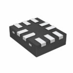 74AVC1T1022GUX
The activity of extra discounts on wholesale prices is in full swing…
Please fill in your contact information and we will send you the latest wholesale price list.





