 ChipApex | Global Electronic Components Supplier
SEARCH
Search Product
Search Post
— IC芯片 | 连接器 | 传感器 | 被动器件 —
Search productSearch post
— IC芯片 | 连接器 | 传感器 | 被动器件 —
Consult the customer manager about the wholesale price.
consultation hotline:86-132-6715-2157
email:[email protected]
Contact the product manager for consultation. One-stop consultation is available.
Do you want a lower wholesale price? Please send us your inquiry and we will reply immediately.
The Diodes Incorporated 74AVC1T45FW5-7 is a single-bit dual power supply translating transceiver with 3-state outputs, housed in an X1-DFN1010-6 package. It supports voltage levels from 1.2V to 3.6V on both VCCA and VCCB rails. The device features a direction control pin (DIR) referenced to VCCA that dictates data flow between pins A and B. Key electrical parameters include a typical propagation delay of 2.8 ns at 3.3V, a maximum operating temperature of +85°C, and a low quiescent current of 20 µA. It provides ±12mA output drive capability and includes IOFF functionality for partial-power-down isolation.
Verify the specific ordering suffix FW5 corresponds to the X1-DFN1010-6 package when sourcing. Confirm RoHS compliance and lead-free status requirements against project specifications. Ensure the tape and reel packaging quantity matches production needs. Check for any recent product change notices regarding marking or material composition updates.
Select this component when a single bidirectional channel with explicit direction control is required. The X1-DFN1010-6 package offers a compact footprint suitable for space-constrained designs. Ensure the application operates within the specified -40°C to +85°C temperature range. Verify that the 3-state output behavior aligns with system bus requirements during power transitions.
This part belongs to the 74AVC1T45 family of translating transceivers manufactured by Diodes Incorporated. The AVC series is designed for low-voltage applications ranging from 1.2V to 3.6V. The FW5 suffix specifically identifies the X1-DFN1010-6 surface-mount package variant within the broader product line.
The datasheet lists the SOT26 package (74AVC1T45W6-7) as a direct chip-scale alternative. Other package variants within the same logical function include FW3, FZ4, and DW. Verify pinout compatibility before substituting with these physical package variations.
The DIR pin is referenced to VCCA. When DIR is high, Pin A acts as the input and Pin B as the output. When DIR is low, the roles reverse, making Pin A the output and Pin B the input.
IOFF forces the outputs into a high-impedance state when either VCCA or VCCB is at 0V. This prevents damaging backflow currents and provides electrical isolation up to 3.6V during partial power-down modes.
Yes, the inputs are designed to accept up to 4.6V, allowing them to interface with higher voltage domains even if the local supply rail is lower.
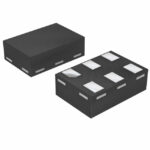 74AVC1T45FW5-7
The activity of extra discounts on wholesale prices is in full swing…
Please fill in your contact information and we will send you the latest wholesale price list.





