 ChipApex | Global Electronic Components Supplier
SEARCH
Search Product
Search Post
— IC芯片 | 连接器 | 传感器 | 被动器件 —
Search productSearch post
— IC芯片 | 连接器 | 传感器 | 被动器件 —
Consult the customer manager about the wholesale price.
consultation hotline:86-132-6715-2157
email:[email protected]
Contact the product manager for consultation. One-stop consultation is available.
Do you want a lower wholesale price? Please send us your inquiry and we will reply immediately.
The Nexperia 74AVC4T3144GU12-QX is a 4-bit dual-supply level translating buffer with 3-state outputs, qualified to AEC-Q100 Grade 1. It translates three inputs from VCC(A) to VCC(B) and one input from VCC(B) to VCC(A). Supply voltages range from 0.8 V to 3.6 V for both ports. Maximum data rates reach 380 Mbit/s for translations between 1.8 V and 3.3 V. The device operates within an ambient temperature range of -40 °C to +125 °C and utilizes a 12-terminal XQFN package.
Verify the specific ordering suffix against official Nexperia documentation to confirm package type and temperature range. Ensure the component matches the required automotive grade specifications. Confirm pinout compatibility with the target PCB footprint before integration. Cross-reference the manufacturer part number with authorized distributor listings to validate authenticity.
Select this component for designs requiring asymmetric voltage translation between low-voltage logic domains. Verify that the operating voltage ranges of connected devices fall within the specified 0.8 V to 3.6 V limits. Consider the propagation delay characteristics relative to the target data rate. Ensure the design accommodates the required ESD protection levels for the application environment.
This device belongs to the Nexperia 74AVC series, which features Advanced Very-low-voltage CMOS technology. The series is designed for high-speed applications in low-voltage environments. The QX suffix indicates the specific XQFN12 packaging variant suitable for space-constrained surface-mount assemblies.
Check for direct substitutes within the 74AVC4T3144 family offering different package options. Verify equivalent AEC-Q100 qualification status if automotive reliability is mandatory. Ensure functional parity regarding the asymmetric channel configuration.
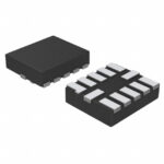 74AVC4T3144GU12-QX
The activity of extra discounts on wholesale prices is in full swing…
Please fill in your contact information and we will send you the latest wholesale price list.




