 ChipApex | Global Electronic Components Supplier
SEARCH
Search Product
Search Post
— IC芯片 | 连接器 | 传感器 | 被动器件 —
Search productSearch post
— IC芯片 | 连接器 | 传感器 | 被动器件 —
Consult the customer manager about the wholesale price.
consultation hotline:86-132-6715-2157
email:[email protected]
Contact the product manager for consultation. One-stop consultation is available.
Do you want a lower wholesale price? Please send us your inquiry and we will reply immediately.
The Nexperia 74AVC4TD245BQ-Q10X is a 4-bit dual supply translating transceiver with configurable voltage translation and 3-state outputs. It features eight 1-bit input-output ports (An and Bn), four direction control inputs (DIR1–DIR4), an output enable input (OE), and dual supply pins (VCC(A) and VCC(B)). Both supplies operate between 0.8 V and 3.6 V, enabling translation between low voltage nodes including 0.8 V, 1.2 V, 1.5 V, 1.8 V, 2.5 V, and 3.3 V. The device supports maximum data rates up to 380 Mbit/s for translations from ≥1.8 V to 3.3 V. It includes IOFF circuitry for partial power-down applications and suspend mode functionality.
Verify the component matches the specific automotive grade requirement by confirming the Q100 suffix indicates AEC-Q100 Grade 1 qualification. Ensure the DHVQFN16 package variant aligns with PCB layout constraints. Confirm that the operating temperature range of -40 °C to +125 °C meets system thermal specifications. Validate that the dual supply voltage limits are compatible with the target application's power rails before integration.
Select this component when designing systems requiring bidirectional translation between multiple low-voltage logic levels within the 0.8 V to 3.6 V range. It is suitable for applications needing individual direction control per bit via DIR inputs. Consider the device if partial power-down isolation is required using IOFF features. Verify that the maximum data rate requirements for specific voltage combinations fall within the specified limits provided in the dynamic characteristics tables.
This part belongs to the 74AVC4TD245-Q100 family of 4-bit dual supply translating transceivers. It is manufactured by Nexperia and utilizes the SOT763-1 package designation. The marking code for identification on the component body is 4TD245. It is designed as a CMOS logic device compliant with JEDEC standards for various supply voltage ranges.
Public confirmed substitute part numbers: None identified in source material.
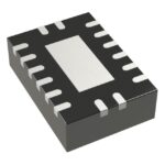 74AVC4TD245BQ-Q10X
The activity of extra discounts on wholesale prices is in full swing…
Please fill in your contact information and we will send you the latest wholesale price list.





