 ChipApex | Global Electronic Components Supplier
SEARCH
Search Product
Search Post
— IC芯片 | 连接器 | 传感器 | 被动器件 —
Search productSearch post
— IC芯片 | 连接器 | 传感器 | 被动器件 —
Consult the customer manager about the wholesale price.
consultation hotline:86-132-6715-2157
email:[email protected]
Contact the product manager for consultation. One-stop consultation is available.
Do you want a lower wholesale price? Please send us your inquiry and we will reply immediately.
The NXP USA Inc. 74AVCM162835DGG:11 is an 18-bit universal bus driver housed in a 56-pin TSSOP package. It operates on a supply voltage range of 1.2 V to 3.6 V and supports input/output tolerance up to 3.6 V. The device features integrated 15 Ω termination resistors to minimize signal overshoot and undershoot, ensuring high-speed data transfer with low power consumption.
Verify the manufacturer origin as Philips Semiconductors or NXP. Confirm the package type is 56-pin TSSOP Type II (SOT364-1). Ensure the temperature range matches -40 °C to +85 °C. Check RoHS compliance status against current environmental regulations before procurement.
Select this component for designs requiring fast propagation delay and minimal power consumption. It is suitable for live insertion scenarios when OE is tied to VCC via a pullup resistor. Ensure the application utilizes compatible clock distribution devices like PCK2510S for optimal performance.
This part belongs to the 74AVCM logic family, designed for high-speed digital applications. It functions as a registered driver with latch enable and clock inputs. The device is intended to reduce signal loads on memory controllers and prevent timing delays in complex digital systems.
Check for direct equivalents within the 74AVCM series. Verify pin compatibility and electrical characteristics if substituting with other 18-bit registered drivers. Ensure the replacement supports the required 1.2 V to 3.6 V operating range.
The OE input should be tied to VCC through a pullup resistor to ensure the high-impedance state during power-up or power-down.
The maximum clock pulse frequency varies by voltage; it is 500 MHz at 3.3 V, 400 MHz at 2.5 V, and 250 MHz at 1.8 V.
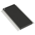 74AVCM162835DGG:11
The activity of extra discounts on wholesale prices is in full swing…
Please fill in your contact information and we will send you the latest wholesale price list.





