 ChipApex | Global Electronic Components Supplier
SEARCH
Search Product
Search Post
— IC芯片 | 连接器 | 传感器 | 被动器件 —
Search productSearch post
— IC芯片 | 连接器 | 传感器 | 被动器件 —
Consult the customer manager about the wholesale price.
consultation hotline:86-132-6715-2157
email:[email protected]
Contact the product manager for consultation. One-stop consultation is available.
Do you want a lower wholesale price? Please send us your inquiry and we will reply immediately.
The NXP USA Inc. 74AVCM162835DGG,11 is an 18-bit registered driver featuring integrated 15 Ω termination resistors and 3-state outputs. It operates on a wide supply voltage range of 1.2 V to 3.6 V and complies with JEDEC standards. The device utilizes a 56-pin TSSOP package (SOT364-1) and supports an operating temperature range from -40 °C to +85 °C. Designed for low power consumption, it includes multiple VCC and GND pins to minimize noise and ground bounce.
Verify the component status as this part may be obsolete or subject to discontinuation notices. Confirm that the specific ordering code matches the required package type and temperature range. Ensure compatibility with existing JEDEC standards and voltage requirements before finalizing procurement decisions.
Select this component for high-speed data transmission requiring precise signal integrity through integrated termination. Consider the 18-bit width and registered output capabilities for complex bus architectures. Evaluate the low inductance design benefits for noise-sensitive environments and ensure the 3-state functionality aligns with system control logic.
This component belongs to the AVCM series of universal bus drivers designed for high-performance digital applications. It serves as a registered driver solution, providing latched outputs controlled by clock and latch enable inputs. The integration of termination resistors distinguishes it from standard buffer devices, offering enhanced signal quality for memory interfaces.
Consult official replacement lists for discontinued parts. Verify pinout and electrical specifications against potential substitutes to ensure functional equivalence without redesigning the host circuit board.
The device supports partial power-down applications using IOFF circuitry, which disables outputs to prevent damaging backflow currents when powered down.
The Latch Enable (LE) input controls the latching of data from the A inputs to the internal register, allowing data to be held stable at the outputs independent of the clock input.
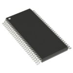 74AVCM162835DGG,11
The activity of extra discounts on wholesale prices is in full swing…
Please fill in your contact information and we will send you the latest wholesale price list.





