 ChipApex | Global Electronic Components Supplier
SEARCH
Search Product
Search Post
— IC芯片 | 连接器 | 传感器 | 被动器件 —
Search productSearch post
— IC芯片 | 连接器 | 传感器 | 被动器件 —
Consult the customer manager about the wholesale price.
consultation hotline:86-132-6715-2157
email:[email protected]
Contact the product manager for consultation. One-stop consultation is available.
Do you want a lower wholesale price? Please send us your inquiry and we will reply immediately.
The Nexperia 74CB3Q3253PWJ is a dual high-bandwidth single-pole, quad-throw FET bus switch housed in a TSSOP16 package. It features an internal charge pump that increases the gate voltage of the NMOS pass transistor, enabling improved RON and RON(flat) performance. This architecture allows the device to switch 5 V signals even when operating at a VCC of 3.3 V. The component supports a wide supply voltage range from 2.3 V to 3.6 V and operates within a temperature range of -40 °C to +85 °C.
Verify the specific suffix 'PWJ' against official Nexperia documentation to confirm exact tape-and-reel packaging specifications and lot traceability requirements. Ensure the procurement channel provides valid manufacturer authorization. Confirm that the delivered components match the TSSOP16 (SOT403-1) package outline dimensions specified in the datasheet to prevent assembly issues.
Select this component when designing circuits requiring the translation or switching of 5 V logic levels using a lower 3.3 V control supply. The integrated charge pump eliminates the need for external level-shifting components. Consider the low OFF-state capacitance for high-frequency applications where signal integrity is critical. Verify that the required ON resistance characteristics meet the specific load current demands of the target application.
This part belongs to the 74CB3Q series of FET bus switches manufactured by Nexperia. These devices are designed for high-speed data routing and signal conditioning in digital systems. The 74CB3Q3253 variant specifically provides two independent 1-of-4 multiplexer/demultiplexer channels, offering flexible routing options for complex bus architectures.
Check for direct pin-compatible substitutes such as the 74CB3Q3253BQ in DHVQFN16 package if space constraints differ. Verify functional equivalence regarding the charge pump mechanism and maximum switching voltages before substituting.
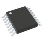 74CB3Q3253PWJ
The activity of extra discounts on wholesale prices is in full swing…
Please fill in your contact information and we will send you the latest wholesale price list.






