 ChipApex | Global Electronic Components Supplier
SEARCH
Search Product
Search Post
— IC芯片 | 连接器 | 传感器 | 被动器件 —
Search productSearch post
— IC芯片 | 连接器 | 传感器 | 被动器件 —
Consult the customer manager about the wholesale price.
consultation hotline:86-132-6715-2157
email:[email protected]
Contact the product manager for consultation. One-stop consultation is available.
Do you want a lower wholesale price? Please send us your inquiry and we will reply immediately.
The Nexperia 74CB3Q3257BQX is a quad high-bandwidth single-pole, double-throw FET bus switch featuring an internal charge pump. It operates on a single supply voltage ranging from 2.3 V to 3.6 V and supports overvoltage switching of signals up to 5 V when powered by 2.5 V or 3.3 V. The device provides four independent channels with one select input (S) and one output enable input (OE). It utilizes a DHVQFN16 package.
Verify the specific ordering suffix 'X' against official Nexperia documentation to confirm tape-and-reel packaging specifications. Confirm that the DHVQFN16 package variant matches the required thermal and mechanical constraints for the target PCB layout. Ensure compatibility with the -40 °C to +85 °C operating temperature range specified in the product data sheet.
Select this component when interfacing between different voltage domains requiring bidirectional signal routing. The integrated charge pump makes it suitable for applications where low supply voltage must control higher voltage signal paths. Consider the low ON resistance and capacitance characteristics for maintaining signal integrity in high-speed digital buses.
This part belongs to the 74CB3Q series of FET bus switches designed for high-performance signal routing. It shares functional similarities with other 74CBTLV and CBT families but distinguishes itself through the inclusion of a charge pump for enhanced overvoltage tolerance. The BQ suffix indicates the DHVQFN16 leadless package format.
An internal charge pump increases the gate voltage of the NMOS pass transistor, allowing the switch to handle 5 V signals even when the supply voltage is only 2.5 V or 3.3 V.
The Output Enable (OE) pin controls the state of the switches. When OE is HIGH, all switches are disabled (high-impedance OFF-state). When OE is LOW, the switches are enabled and controlled by the S input.
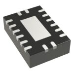 74CB3Q3257BQX
The activity of extra discounts on wholesale prices is in full swing…
Please fill in your contact information and we will send you the latest wholesale price list.





