 ChipApex | Global Electronic Components Supplier
SEARCH
Search Product
Search Post
— IC芯片 | 连接器 | 传感器 | 被动器件 —
Search productSearch post
— IC芯片 | 连接器 | 传感器 | 被动器件 —
Consult the customer manager about the wholesale price.
consultation hotline:86-132-6715-2157
email:[email protected]
Contact the product manager for consultation. One-stop consultation is available.
Do you want a lower wholesale price? Please send us your inquiry and we will reply immediately.
The onsemi 74F299SC is an octal universal shift/storage register housed in a 20-lead SOIC package. It features eight edge-triggered D-type flip-flops with common parallel I/O pins and 3-state outputs. The device supports four operating modes: hold, shift left, shift right, and parallel load. Key electrical parameters include a maximum clock frequency of 85 MHz at 0°C to +70°C, propagation delays ranging from 4.0 ns to 10.0 ns depending on the mode and temperature, and a supply voltage range of 4.5V to 5.5V. It includes an active LOW master reset and guarantees 4000V minimum ESD protection.
Verify the specific package variant, as the 74F299 series is available in SOIC, SOP, and PDIP packages. Confirm that the component meets the required ambient temperature range of 0°C to +70°C for your application. Ensure compatibility with 5V logic levels and check for any end-of-life status or obsolescence notices from the manufacturer before finalizing procurement plans.
Select this component when an octal register with bidirectional shifting and common I/O is required. It is suitable for designs needing 3-state output isolation on a shared bus. Consider the propagation delay specifications relative to your system clock speed. Verify that the 20-lead package format fits your PCB layout constraints compared to other logic families.
The 74F299 belongs to the Fairchild/ON Semiconductor 74F logic family, known for high-speed performance. This specific part is an octal universal shift/storage register. The 'SC' suffix denotes the 20-lead Small Outline Integrated Circuit (SOIC) package. It was originally manufactured by Fairchild Semiconductor Corporation before the company's acquisition by ON Semiconductor.
Direct substitutes may include other octal universal shift registers from the 74F series or compatible logic families such as 74LS299, though electrical characteristics like speed and drive current will differ. Verify pinout compatibility and 3-state functionality when selecting alternatives.
The parallel load inputs and flip-flop outputs are multiplexed to common I/O pins to reduce the total number of package pins required.
The operation mode is determined by the logic levels on the S0 and S1 select inputs, which control whether the device holds, shifts left, shifts right, or loads data.
The 3-state outputs are disabled by HIGH signals on either OE1 or OE2, putting the I/O pins in a high impedance state, or by HIGH signals on both S0 and S1 during parallel load preparation.
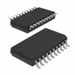 74F299SC
The activity of extra discounts on wholesale prices is in full swing…
Please fill in your contact information and we will send you the latest wholesale price list.





