 ChipApex | Global Electronic Components Supplier
SEARCH
Search Product
Search Post
— IC芯片 | 连接器 | 传感器 | 被动器件 —
Search productSearch post
— IC芯片 | 连接器 | 传感器 | 被动器件 —
Consult the customer manager about the wholesale price.
consultation hotline:86-132-6715-2157
email:[email protected]
Contact the product manager for consultation. One-stop consultation is available.
Do you want a lower wholesale price? Please send us your inquiry and we will reply immediately.
The onsemi 74F322PC is an octal serial/parallel register with sign extend functionality, belonging to the 74F logic series. It features multiplexed parallel I/O ports and separate serial input/output lines. The device operates within a supply voltage range of +4.5V to +5.5V and supports a maximum clock frequency of 90 MHz at +25°C. It provides three-state outputs for bus applications and includes an asynchronous Master Reset input. The component is housed in a 20-lead plastic dual-in-line package (PDIP) suitable for through-hole mounting.
Verify component authenticity and datasheet revision status before integration. Confirm that the PDIP-20 package dimensions match your PCB footprint requirements. Check for RoHS compliance documentation if environmental regulations apply to your manufacturing process. Ensure that the discontinued status does not conflict with long-term production lifecycle requirements.
Select this component when an octal register with specific sign extend capabilities is required for arithmetic operations. The 74F series offers high-speed performance suitable for demanding timing constraints. Consider the multiplexed I/O architecture if pin count reduction is critical. Verify that the bipolar logic family characteristics align with your system's power and noise immunity specifications.
The 74F322 is part of the Fairchild Semiconductor 74F logic family, designed for high-speed digital applications. It serves as an octal shift register with specialized features for arithmetic processing. The device integrates eight D-type edge-triggered flip-flops with interstage gating for shift operations and intrastage gating for parallel loading. It represents a specialized solution for data manipulation in complex digital systems.
No public confirmed substitute part numbers are available in the provided documentation.
When the SE input is LOW during a shift right operation, Q7 reloads its previous contents, effectively extending the sign bit for two's complement arithmetic.
The OE (Output Enable) input controls the three-state buffers. A HIGH signal on OE disables the outputs, placing them in a high-impedance state regardless of other control inputs.
Yes, parallel loading occurs on the rising edge of the clock pulse when RE is LOW and S/P is LOW, allowing synchronous data entry from the multiplexed I/O terminals.
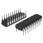 74F322PC
The activity of extra discounts on wholesale prices is in full swing…
Please fill in your contact information and we will send you the latest wholesale price list.





