 ChipApex | Global Electronic Components Supplier
SEARCH
Search Product
Search Post
— IC芯片 | 连接器 | 传感器 | 被动器件 —
Search productSearch post
— IC芯片 | 连接器 | 传感器 | 被动器件 —
Consult the customer manager about the wholesale price.
consultation hotline:86-132-6715-2157
email:[email protected]
Contact the product manager for consultation. One-stop consultation is available.
Do you want a lower wholesale price? Please send us your inquiry and we will reply immediately.
The Renesas Electronics 74FCT3807APYGI is a low skew, single-input to ten-output LVCMOS clock buffer. It operates within a supply voltage range of 1.8V to 3.6V and supports maximum frequencies up to 100 MHz. The device features an additive phase jitter of less than 50 fs. It is housed in a 20-pin SSOP package with dimensions of 7.2mm x 5.3mm x 1.7mm and a lead pitch of 0.65mm. The component is designed for surface-mount installation and complies with RoHS standards.
Verify the specific suffix 'I' against official Renesas documentation to confirm industrial temperature rating (-40°C to 85°C) versus commercial variants. Confirm package type compatibility, as the base model may be available in QSOP or TSSOP. Check current lifecycle status and availability through authorized distributors, as production schedules vary by region.
Select this component when sub-50fs jitter performance is critical for signal integrity. Ensure the design requires a 1:10 fan-out ratio. Verify that the PCB layout accommodates the 20-SSOP footprint. Compare against other 74FCT3807 variants if different packaging options like VFQFPN are preferred for space constraints.
This part belongs to the 74FCT3807 family of clock buffers. Related variants include the 74FCT3807AQG8 and 74FCT3807SPYGI8. These components share similar electrical characteristics but differ in packaging, temperature ranges, and specific output drive capabilities. The family is designed for high-performance clock distribution applications.
Direct pin-to-pin replacements within the same family include 74FCT3807AQG and 74FCT3807QG. Cross-manufacturer alternatives such as onsemi NB3V8312CMNR4G may offer similar functionality but require verification of electrical parameters and pinout compatibility.
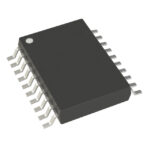 74FCT3807APYGI
The activity of extra discounts on wholesale prices is in full swing…
Please fill in your contact information and we will send you the latest wholesale price list.






