 ChipApex | Global Electronic Components Supplier
SEARCH
Search Product
Search Post
— IC芯片 | 连接器 | 传感器 | 被动器件 —
Search productSearch post
— IC芯片 | 连接器 | 传感器 | 被动器件 —
Consult the customer manager about the wholesale price.
consultation hotline:86-132-6715-2157
email:[email protected]
Contact the product manager for consultation. One-stop consultation is available.
Do you want a lower wholesale price? Please send us your inquiry and we will reply immediately.
The SN74GTLP2034 is an 8-bit LVTTL-to-GTLP adjustable-edge-rate registered transceiver with a split LVTTL port and feedback path. It operates at VCC = 3.3V (3.15V to 3.45V) and supports GTLP termination voltages of 1.5V (VTT) and reference voltage of 1V (VREF). The device provides high-drive GTLP open-drain outputs capable of sourcing up to 100 mA, while LVTTL outputs provide -24 mA/24 mA drive. It features variable edge-rate control (ERC), Ioff, power-up 3-state, and BIAS VCC for live insertion support. Operating temperature range is -40°C to +85°C.
Verify the specific package variant (DGG or DGV) and tape-and-reel suffix (R) against the required form factor. Confirm that the design environment supports the specified GTLP termination voltage (VTT = 1.5 V) and reference voltage (VREF = 1 V). Ensure that the ERC pin is properly biased to achieve the desired edge rate for signal integrity. Check for availability as this component may be subject to discontinuation or lifecycle changes.
Select this transceiver when a true logic translation between LVTTL and GTLP domains is required, rather than simple buffering. The split A-port (AI and AO) is essential if diagnostic feedback of the transmitted data is needed on the local board. Consider the ERC feature if system signal integrity requires optimization of rise/fall times for heavily loaded backplanes. Verify that the 100 mA drive capability matches the backplane impedance requirements.
This component belongs to Texas Instruments' Widebus family, designed for high-performance bus interfacing. It utilizes TI-OPC circuitry to limit ringing on unevenly loaded backplanes and OEC circuitry to improve signal integrity. The device serves as a bridge between standard LVTTL logic devices and high-speed GTLP backplane architectures, offering registered data transfer modes including buffer, latch, and flip-flop configurations.
SN74GTLP2034DGGR
The SN74GTLP2034 supports live insertion through Ioff circuitry, which disables outputs during power-down; Power-Up 3-State circuitry, which places outputs in a high-impedance state during power transitions; and BIAS VCC circuitry, which precharges the B-port connections to prevent disturbance of active data.
The Variable Edge-Rate Control (ERC) input allows the designer to adjust the B-port output rise and fall times. Setting ERC high results in slow edge rates, while setting it low results in fast edge rates, enabling optimization of data-transfer rates and signal integrity for distributed loads.
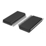 74GTLP2034DGGRE4
The activity of extra discounts on wholesale prices is in full swing…
Please fill in your contact information and we will send you the latest wholesale price list.






