 ChipApex | Global Electronic Components Supplier
SEARCH
Search Product
Search Post
— IC芯片 | 连接器 | 传感器 | 被动器件 —
Search productSearch post
— IC芯片 | 连接器 | 传感器 | 被动器件 —
Consult the customer manager about the wholesale price.
consultation hotline:86-132-6715-2157
email:[email protected]
Contact the product manager for consultation. One-stop consultation is available.
Do you want a lower wholesale price? Please send us your inquiry and we will reply immediately.
The SN74GTLP22034 is an 8-bit LVTTL-to-GTLP adjustable-edge-rate registered transceiver with a split LVTTL port and feedback path. It operates at VCC = 3.3 V (3.15–3.45 V) and supports GTL (VTT = 1.2 V, VREF = 0.8 V) or GTLP (VTT = 1.5 V, VREF = 1 V). The device provides high-drive GTLP outputs (IOL = 100 mA) and standard LVTTL outputs (±12 mA). It features configurable buffer, latch, and flip-flop modes via IMODE/OMODE inputs, with clock frequencies up to 175 MHz. Propagation delays range from 1 ns to 8.7 ns depending on mode and edge rate.
Verify the exact ordering suffix against the manufacturer's current documentation. The DGV package corresponds to the TVSOP-48 form factor. Confirm that the specific revision level matches your design requirements, as datasheet parameters are subject to change without notice. Ensure compatibility with your system's termination voltage and reference voltage specifications before finalizing procurement.
Select this component when a registered transceiver is required to bridge LVTTL logic domains with GTLP backplane signaling. The inclusion of ERC allows optimization of signal integrity under varying distributed load conditions. The split A-port architecture is essential for designs requiring simultaneous transparent data flow and diagnostic feedback monitoring. Verify that the 100 mA drive capability meets the impedance requirements of the target backplane.
This device belongs to Texas Instruments' Widebus family of high-drive bus transceivers. It shares functional similarities with the SN74FB2033 but implements true GTLP logic rather than buffered TTL. The SN74GTLP22034 is designed specifically for high-speed backplane applications where signal integrity and live insertion capabilities are critical constraints.
SN74GTLP22034DGVR
Changing the ERC input voltage adjusts the B-port output rise and fall times. Setting ERC high results in slow edge rates, while setting it low results in fast edge rates, allowing designers to optimize data-transfer rates and signal integrity.
The separate AI and AO pins provide a feedback path for control and diagnostics monitoring, allowing the system to verify data transmission status independently of the main output path.
Yes, the device is fully specified for live-insertion applications through the use of Ioff circuitry, power-up 3-state functionality, and BIAS VCC precharge circuitry to prevent damage and data disturbance during card insertion.
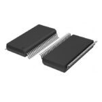 74GTLP22034DGGRE4
The activity of extra discounts on wholesale prices is in full swing…
Please fill in your contact information and we will send you the latest wholesale price list.






